Difference between revisions of "Soft Lithography"
| (9 intermediate revisions by the same user not shown) | |||
| Line 1: | Line 1: | ||
[[Category:Lithography]] [[Category:Soft Lithography]] | [[Category:Lithography]] [[Category:Soft Lithography]] | ||
__NOTOC__ | __NOTOC__ | ||
| − | + | ||
| + | ==About== | ||
Soft lithography is the transfer of patterned microstructures with molded elastomer. The most common elastomer used in this technique is PDMS (polydimethylsiloxane), which is <u>soft</u>, low cost and easy to mold. It is also bio-compatible with high thermal stability and high chemical stability, is chemically inert, insulating, transparent to UV and visible light, mechanically flexible and durable, allowing many applications. The most common devices fabricated with this technique are microfluidics. <br> | Soft lithography is the transfer of patterned microstructures with molded elastomer. The most common elastomer used in this technique is PDMS (polydimethylsiloxane), which is <u>soft</u>, low cost and easy to mold. It is also bio-compatible with high thermal stability and high chemical stability, is chemically inert, insulating, transparent to UV and visible light, mechanically flexible and durable, allowing many applications. The most common devices fabricated with this technique are microfluidics. <br> | ||
<u><small>'''NOTE</u>:'''</small> You might hear soft lithography equated to "microfluidics fabrication." However, it is important to remember that not all microfluidic devices are fabricated by soft lithography and not all soft lithography is for microfluidic applications! | <u><small>'''NOTE</u>:'''</small> You might hear soft lithography equated to "microfluidics fabrication." However, it is important to remember that not all microfluidic devices are fabricated by soft lithography and not all soft lithography is for microfluidic applications! | ||
| − | + | ==Process Flow== | |
| − | *The master used can be fabricated out of photoresist or etched silicon. The most commonly used materials are epoxy-based negative photoresist (SU8 | + | [[File: SoftLitho Protocol Oct2025.PNG|thumb|right|upright=1.75|'''Standard QNF Soft Lithography Protocol, Updated May 2025.''' <br>Images from [https://www.fabublox.com/process-editor/70e6195b-900a-48e8-8b05-70dd807d973f "Microfluidics at QNF" Process on Fabublox] ]] |
| + | *The master used can be fabricated out of photoresist or etched silicon. The most commonly used materials are epoxy-based negative photoresist (SU8 / HARE SQ). For a negative photoresist, the parts exposed to UV become cross-linked, while the remainder of the film remains soluble and can be washed away during development. The height of this structure is determined by the thickness of the resist, which we control through our application method. The length and width of features are patterned through the UV exposure, either by mask or direct write tools.<br> | ||
*For molding success, there are two important components to think about -- master durability and PDMS removal. Etched silicon molds will be more durable than patterned photoresist. However, an O2 plasma treatment under vacuum before applying resist has shown more than sufficient adhesion for patterned HARE SQ in our own tests. To enable easy release of the PDMS from the mold, it can be beneficial to do a silanization treatment before applying the PDMS.<br> | *For molding success, there are two important components to think about -- master durability and PDMS removal. Etched silicon molds will be more durable than patterned photoresist. However, an O2 plasma treatment under vacuum before applying resist has shown more than sufficient adhesion for patterned HARE SQ in our own tests. To enable easy release of the PDMS from the mold, it can be beneficial to do a silanization treatment before applying the PDMS.<br> | ||
*An O2 plasma step is included if applying the PDMS to glass or another piece of PDMS to make a device. | *An O2 plasma step is included if applying the PDMS to glass or another piece of PDMS to make a device. | ||
| − | + | ====QNF Standard Protocols==== | |
| − | * [https://wiki.nano.upenn.edu/wiki/images/c/cf/Microfluidics_Process_Flow.pdf Making a Master | + | * [https://www.fabublox.com/process-editor/70e6195b-900a-48e8-8b05-70dd807d973f Complete Process on Fabublox] |
| − | * Making a Device: PDMS to PDMS bonding | + | * [https://wiki.nano.upenn.edu/wiki/images/9/9d/SoftLitho_Protocol_Oct2025.PNG Making a Master - visual overview] |
| − | + | * [https://wiki.nano.upenn.edu/wiki/images/c/cf/Microfluidics_Process_Flow.pdf Making a Master - detailed instructions] | |
| + | * [https://wiki.nano.upenn.edu/wiki/images/0/0c/SOP_Microfluidics.pdf Making a Device: PDMS to PDMS bonding] | ||
| − | =====Videos | + | =====Tips & Tricks===== |
| + | * Be sure to mix the PDMS base and curing agent together VERY well for ~5 minutes! If not mixed well, the cured PDMS may adhere to the master and ruin it. | ||
| + | * An aluminum tray that can accommodate a wafer is a very helpful container for applying the PDMS -- available in the [https://nemo.nano.upenn.edu/stockroom/ QNF Stockroom] | ||
| + | * A 1mm biopsy punch is a great way to add inlet/outlet ports. We have these available for use in our PDMS room. | ||
| + | * A main cause of failure of the master is cracking of the wafer. Be careful not to score the wafer when cutting out your devices! | ||
| + | * A drop of IPA can be a helpful lubricant when cutting and removing the PDMS mold can be very helpful. | ||
| + | * Trying to remove the wafer from the PDMS mold can easily crack the wafer. It is easier to cut out only the devices needed. | ||
| + | * Applying trichloro(1H, 1H, 2H, 2H-perfluoro-octyl) silane in a vacuum desiccator before applying PDMS can make it easier to remove the mold from the master. This is really only necessary if there are small features with high aspect ratios. | ||
| + | |||
| + | ====Videos==== | ||
* [https://www.youtube.com/watch?v=ybFHtd2pPYs Spin Coating Thick Resist] | * [https://www.youtube.com/watch?v=ybFHtd2pPYs Spin Coating Thick Resist] | ||
* [https://www.youtube.com/watch?v=SCs87pYIn5w Negative Resist First Mask Alignment Mark] | * [https://www.youtube.com/watch?v=SCs87pYIn5w Negative Resist First Mask Alignment Mark] | ||
| Line 21: | Line 33: | ||
* [https://www.youtube.com/watch?v=powcV3r4IhM Degassing PDMS] | * [https://www.youtube.com/watch?v=powcV3r4IhM Degassing PDMS] | ||
| − | =====Related | + | ==Equipment at QNF== |
| + | <u><small>'''NOTE</u>:'''</small> To minimize contamination, we have a separate room within the Soft Materials area dedicated to PDMS mixing and molding. Uncured PDMS may not be removed from this room. Cutting PDMS or punching out inlets/outlets must be kept to inside this room or completely outside of the cleanroom. Many researchers use PDMS in their own (non-cleanroom) labs with very satisfactory results. | ||
| + | |||
| + | ==== Soft Materials ==== | ||
| + | * '''DE-07:''' [[Anatech SCE-106 Barrel Asher | Anatech SCE-106 Barrel Asher]] | ||
| + | * '''MA-03:''' [[ABM Mask Aligner | ABM Mask Aligner]] | ||
| + | * '''PVD-08:''' Silanization Dessicator | ||
| + | * '''SPN-08:''' [[ CEE Apogee Spinner | CEE Apogee Spinner - Negative Epoxy]] | ||
| + | * '''SPN-09:''' [[ CEE Apogee Spinner | CEE Apogee Spinner - PDMS]] | ||
| + | * '''LW-02:''' [[Nanoscribe Photonic Professional GT | Nanoscribe Photonic Professional GT]] | ||
| + | ==== Main Cleanroom ==== | ||
| + | * '''LW-01:''' [[Heidelberg DWL 66+ Laser Writer | Heidelberg DWL 66+ Laser Writer]] | ||
| + | * '''LW-03:''' [[DMO MicroWriter ML3 Pro | DMO MicroWriter ML3 Pro ]] | ||
| + | * '''MA-01:''' [[SUSS MicroTec MA6 Gen3 Mask Aligner | SUSS MicroTec MA6 Gen3 Mask Aligner]] | ||
| + | * '''DE-03:''' [[SPTS Si DRIE | SPTS Si DRIE]] | ||
| + | |||
| + | ==Want to Know More?== | ||
| + | ====Related Wiki Pages==== | ||
* [[Photolithography]] | * [[Photolithography]] | ||
* [[Resists at QNF]] | * [[Resists at QNF]] | ||
* [[How to Make a Mask]] | * [[How to Make a Mask]] | ||
| − | + | ====Internal Reports & Presentations==== | |
| − | + | * [https://wiki.nano.upenn.edu/wiki/images/a/a8/Sosa_Singh-Poster_2025.pdf Establishing HARE SQ Protocols at QNF -- Delamination Testing of Soft Litho Masters (Poster)] ''Singh Center Annual User Meeting, Oct 2025'' | |
*[https://repository.upenn.edu/entities/publication/ae5bbb10-7b45-4568-9f0f-f2f27e7d95c2 T-Topping Study Report] | *[https://repository.upenn.edu/entities/publication/ae5bbb10-7b45-4568-9f0f-f2f27e7d95c2 T-Topping Study Report] | ||
| − | |||
* [https://upenn.box.com/s/b6e694cf6r5qul32cmsjkbr9oydc6d7o QNF Soft Lithography Workshop Process Flow - SU8 3050] | * [https://upenn.box.com/s/b6e694cf6r5qul32cmsjkbr9oydc6d7o QNF Soft Lithography Workshop Process Flow - SU8 3050] | ||
* [https://upenn.box.com/s/xrlkb6agcqae7ietb16mk5d84zqbcbr0 Presentation for Workshop - Biological Researchers (PDF Format)] | * [https://upenn.box.com/s/xrlkb6agcqae7ietb16mk5d84zqbcbr0 Presentation for Workshop - Biological Researchers (PDF Format)] | ||
* [https://upenn.box.com/s/10wkjldwrt3f6it5ted0jo74b72eu0m4 Presentation for ESE 536 Course Module (PDF Format)] | * [https://upenn.box.com/s/10wkjldwrt3f6it5ted0jo74b72eu0m4 Presentation for ESE 536 Course Module (PDF Format)] | ||
| − | + | ||
| + | ====External Resources==== | ||
*[https://df393c79-ecb8-453c-bf20-359d99bdbc77.filesusr.com/ugd/5b8579_bc178fb3a8fb47828522de434712b455.pdf HARE SQ Dispensing and Handling Techniques - KemLab] | *[https://df393c79-ecb8-453c-bf20-359d99bdbc77.filesusr.com/ugd/5b8579_bc178fb3a8fb47828522de434712b455.pdf HARE SQ Dispensing and Handling Techniques - KemLab] | ||
*[https://piescientific.com/resource-pdms-bonding/ PDMS Bonding - PIE Scientific] | *[https://piescientific.com/resource-pdms-bonding/ PDMS Bonding - PIE Scientific] | ||
*Microfluidics and Nanofluidics Handbook: SU-8 Photolithography and Its Impact on Microfluidics by Rodrigo Martinez-Duarte and Marc J. Madou | *Microfluidics and Nanofluidics Handbook: SU-8 Photolithography and Its Impact on Microfluidics by Rodrigo Martinez-Duarte and Marc J. Madou | ||
Latest revision as of 11:14, 11 November 2025
About
Soft lithography is the transfer of patterned microstructures with molded elastomer. The most common elastomer used in this technique is PDMS (polydimethylsiloxane), which is soft, low cost and easy to mold. It is also bio-compatible with high thermal stability and high chemical stability, is chemically inert, insulating, transparent to UV and visible light, mechanically flexible and durable, allowing many applications. The most common devices fabricated with this technique are microfluidics.
NOTE: You might hear soft lithography equated to "microfluidics fabrication." However, it is important to remember that not all microfluidic devices are fabricated by soft lithography and not all soft lithography is for microfluidic applications!
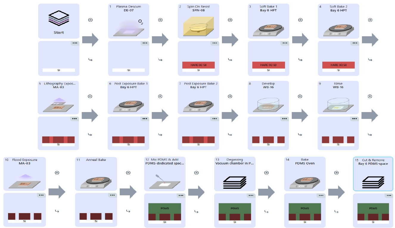
Process Flow

Images from "Microfluidics at QNF" Process on Fabublox
- The master used can be fabricated out of photoresist or etched silicon. The most commonly used materials are epoxy-based negative photoresist (SU8 / HARE SQ). For a negative photoresist, the parts exposed to UV become cross-linked, while the remainder of the film remains soluble and can be washed away during development. The height of this structure is determined by the thickness of the resist, which we control through our application method. The length and width of features are patterned through the UV exposure, either by mask or direct write tools.
- For molding success, there are two important components to think about -- master durability and PDMS removal. Etched silicon molds will be more durable than patterned photoresist. However, an O2 plasma treatment under vacuum before applying resist has shown more than sufficient adhesion for patterned HARE SQ in our own tests. To enable easy release of the PDMS from the mold, it can be beneficial to do a silanization treatment before applying the PDMS.
- An O2 plasma step is included if applying the PDMS to glass or another piece of PDMS to make a device.
QNF Standard Protocols
- Complete Process on Fabublox
- Making a Master - visual overview
- Making a Master - detailed instructions
- Making a Device: PDMS to PDMS bonding
Tips & Tricks
- Be sure to mix the PDMS base and curing agent together VERY well for ~5 minutes! If not mixed well, the cured PDMS may adhere to the master and ruin it.
- An aluminum tray that can accommodate a wafer is a very helpful container for applying the PDMS -- available in the QNF Stockroom
- A 1mm biopsy punch is a great way to add inlet/outlet ports. We have these available for use in our PDMS room.
- A main cause of failure of the master is cracking of the wafer. Be careful not to score the wafer when cutting out your devices!
- A drop of IPA can be a helpful lubricant when cutting and removing the PDMS mold can be very helpful.
- Trying to remove the wafer from the PDMS mold can easily crack the wafer. It is easier to cut out only the devices needed.
- Applying trichloro(1H, 1H, 2H, 2H-perfluoro-octyl) silane in a vacuum desiccator before applying PDMS can make it easier to remove the mold from the master. This is really only necessary if there are small features with high aspect ratios.
Videos
- Spin Coating Thick Resist
- Negative Resist First Mask Alignment Mark
- Developing SU8 Resist
- Degassing PDMS
Equipment at QNF
NOTE: To minimize contamination, we have a separate room within the Soft Materials area dedicated to PDMS mixing and molding. Uncured PDMS may not be removed from this room. Cutting PDMS or punching out inlets/outlets must be kept to inside this room or completely outside of the cleanroom. Many researchers use PDMS in their own (non-cleanroom) labs with very satisfactory results.
Soft Materials
- DE-07: Anatech SCE-106 Barrel Asher
- MA-03: ABM Mask Aligner
- PVD-08: Silanization Dessicator
- SPN-08: CEE Apogee Spinner - Negative Epoxy
- SPN-09: CEE Apogee Spinner - PDMS
- LW-02: Nanoscribe Photonic Professional GT
Main Cleanroom
- LW-01: Heidelberg DWL 66+ Laser Writer
- LW-03: DMO MicroWriter ML3 Pro
- MA-01: SUSS MicroTec MA6 Gen3 Mask Aligner
- DE-03: SPTS Si DRIE
Want to Know More?
Related Wiki Pages
Internal Reports & Presentations
- Establishing HARE SQ Protocols at QNF -- Delamination Testing of Soft Litho Masters (Poster) Singh Center Annual User Meeting, Oct 2025
- T-Topping Study Report
- QNF Soft Lithography Workshop Process Flow - SU8 3050
- Presentation for Workshop - Biological Researchers (PDF Format)
- Presentation for ESE 536 Course Module (PDF Format)
External Resources
- HARE SQ Dispensing and Handling Techniques - KemLab
- PDMS Bonding - PIE Scientific
- Microfluidics and Nanofluidics Handbook: SU-8 Photolithography and Its Impact on Microfluidics by Rodrigo Martinez-Duarte and Marc J. Madou