Nanoscale Characterization Facility
 |
|
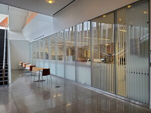
| A view of the sample prep suite from the NCF lobby | |
| Home Institution | University of Pennsylvania |
|---|---|
| Location | Philadelphia, PA |
| Building | Krishna P. Singh Center for Nanotechnology |
| Established | 2013 |
| Director | Douglas Yates |
| Website | https://www.nano.upenn.edu/resources/nanoscale-characterization/ |
About
The Nanoscale Characterization Facility (NCF) supports state-of-the-art tools for electron- and ion-beam analyses for Penn as well as other university, government, and industry users in the Philadelphia region. The facility comprises a suite of rooms specifically designed to host current and next-generation scanning electron, transmission electron, and focused ion beam microscopes. Supplementing these tools is an integrated sample preparation laboratory with sample coating and plasma cleaning capabilities, as well as cryogenic sample preparation equipment and a computer suite for offline image and data analysis. The NCF is currently maintained by three full-time staff scientists with over 45 years of combined experience in materials characterization.
To acknowledge use of NCF facilities in publications, please use the following text:
"This work was performed at the Singh Center for Nanotechnology at the University of Pennsylvania, a member of the National Nanotechnology Coordinated Infrastructure (NNCI) network, which is supported by the National Science Foundation (Grant NNCI-1542153) and through the use of facilities supported by the University of Pennsylvania Materials Research Science and Engineering Center (MRSEC) DMR-2309043."
Access
Instructions for gaining access to the Nanoscale Characterization Facility can be found here.
After establishing an account, go to NEMO Help for information on getting started.
Contact NCF staff to discuss your project needs.
Equipment
Go to NEMO to request training, reserve equipment, and log in to equipment.
Scanning Electron Microscopy
- JEOL 7500F HRSEM | 7500F Reference Guide Image with secondary electrons, backscattered electrons, and transmission electrons at high vacuum and high resolution, even at very low voltages. Elemental analysis with x-rays available with EDS by EDAX.
- TFS Quanta 600 FEG ESEM | Quanta Reference Guide Image non-conductive or vacuum-sensitive specimens in high vacuum or in a low vacuum water vapor environment. EDAX EDS elemental analysis and EBSD crystallography available. This microscope is equipped with a large chamber for in-situ imaging and high- and low-temperature stages.
Focused Ion Beam Microscopy
- TESCAN S8000X FIB/SEM | pFIB SOP A dual beam system with a plasma-source focused ion beam capable of high milling rates and a high resolution electron beam capable of imaging at low energies. This microscope includes an EDAX EDS detector for elemental x-ray analysis and an EBSD camera for crystallographic characterization. Time of Flight Secondary Ion Mass Spectroscopy (ToF-SIMS) enables three dimensional chemical characterization, even of light elements. This microscope is compatible with cryogenic imaging and transfer systems.
- ZEISS Orion NanoFab Helium Ion Microscope | information coming soon
Transmission Electron Microscopy
- JEOL F200 | F2 SOP: NEMO login required A cold field emission transmission electron microscope that can operate at 200kV or 80kV for sensitive specimens. It is equipped with dual EDS detectors, Gatan OneView and Metro cameras, and various apertures for diffraction, darkfield, brightfield, and STEM imaging.
- JEOL NEOARM | NEOARM SOP: NEMO login required This TEM has a highly coherent cold field emission source capable of subangstrom resolutions at both 200kV and 80kV, and is also capable of imaging at 30kV. Equipped with detectors for chemical characterization including EDS and electron energy loss spectrometry (EELS.)
Sample Preparation
- EMS/Quorum Q150T ES Sputter Coater | Coater SOP A user-friendly deposition system for sputter coating metals (typically iridium) or evaporating carbon in thin films onto specimens to improve conductivity for better images and reduced specimen damage.
- Gatan Solarus 950 Advanced Plasma System A plasma cleaning system with ports designed for TEM specimen holders. Equipped with argon, oxygen, and hydrogen gas.