Scanning Electron Microscopy
Overview
Scanning Electron Microscopy (SEM) utilizes a high energy beam of focused electrons to generate images or micrographs of the topographic detail and/or material variation in small specimens. SEMs are capable of few-nanometer resolution with a well-aligned beam and proper sample preparation under appropriate operating conditions. Images are formed by scanning the electron beam point-by-point across a specimen surface. At each point, the beam scatters to generate various signals that are collected then converted to an intensity grayscale and correlated to a pixel.
Equipment
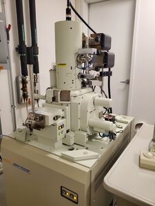
JEOL 7500F HRSEM, now in bay 6
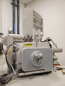
TFS Quanta 600 ESEM in room 004


- JEOL 7500F HRSEM | 7500F Reference Guide Image with secondary electrons, backscattered electrons, and transmission electrons at high vacuum and high resolution, even at very low voltages. Elemental analysis with x-rays available with EDS by EDAX.
- TFS Quanta 600 FEG ESEM | Quanta Reference Guide Image non-conductive or vacuum-sensitive specimens in high vacuum or in a low vacuum water vapor environment. EDAX EDS elemental analysis and EBSD crystallography available. This microscope is equipped with a large chamber for in-situ experiments and high- and low-temperature stages.
Techniques
- EDS - Energy Dispersive X-Ray Spectroscopy: A technique to chemically characterize specimens which collects overview spectra or spectrum maps that can yield an approximate composition of specimens on any of our SEMs.
- EBSD - Electron Backscatter Diffraction: A technique to characterize the crystallographic structure of specimens, preferably specimens that have been polished, to show details such as grain size and orientation. Available on the Quanta.
- Low Voltage SEM - One method to image fine or thin surface details, including on specimens of low to no conductivity. The 7500F is equipped with a gentle beam mode that enables ultra low landing voltages through a stage biasing system.
- Low Vacuum SEM - A charge compensation condition for imaging nonconductive specimens without applying a conductive coating. The Quanta is designed to operate in low vacuum up to 1.5 torr with a water vapor atmosphere. It is also capable of operating at higher pressure, temperature, and humidity in an environmental mode. Humidity at standard low vacuum settings is significantly lower than room humidity and will not adversely affect specimens that can tolerate room air.
Sample Preparation
Contact staff for specific sample preparation advice. We are not a specimen preparation facility; however we can advise on what makes a good specimen and how to mount specimens to stubs for optimal imaging.
General Considerations
- Specimens (and anything going inside the chamber including detectors and specimen holders) should always be handled with gloves.
- Know the sample size limits for the SEM: The Quanta has a large chamber that can accommodate large specimens up to 1kg. The 7500F has a more restrictive chamber: specimens should be no taller than the specimen holder being used, however it can accommodate 4 inch wafers.
- Specimens should be well secured with no loose particles. Contact staff for assistance preparing powder specimens to help prevent contamination or damage inside the chamber.
- Specimens should be clean and vacuum compatible. Outgassing and contamination can both deteriorate the quality of the vacuum and thus diminish the image quality.
Conductivity
- With the exception of the Low Vacuum Mode available on the Quanta, specimens should be conductive for the best image quality. This means creating a conductive pathway from the specimen surface to the stub and stage so that excess electrons can be drawn away from the specimen surface.
- Know the approximate conductivity of your sample: even semiconductors have enough conductivity for good images, but insulators are more difficult and may require additional preparation, such as sputter coating.
- Know the approximate conductivity of your substrates: conductive substrates contribute to the conductive pathway. For instance, Si wafer pieces are easier to image than glass or sapphire.
- All materials provided for sample preparation are conductive, including:
- Double sided carbon tape: Useful for adhering most specimens to stubs or holders, this double sided adhesive is also conductive. Use a small amount for most specimens.
- Single sided copper tape: Useful for adding a conductive pathway to e.g. nonconductive films on conductive substrates. Place copper tape so it is in contact with the specimen of interest and the stub or holder. Ensure that the copper tape is pressed firmly onto the specimen and stub.
- Pin stubs: Stubs are small pieces of aluminum for mounting common specimens. Pin stubs have a pin on the end for secure loading onto specimen holders or stages. Pin stubs come in a variety of forms, including common flat stubs, large area stubs, cross section, intermediate angles, and more.
- Specimen holders: Hold either pin stubs or specimens directly. Some holders also have pins for easy loading. Others have large areas and unique geometry or mechanics to hold large or odd shaped specimens.
- Stub preparation examples

A simple preparation method.
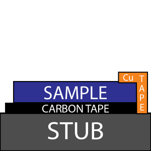
For non-conductive specimens, especially non-conductive specimens on a conductive substrate.
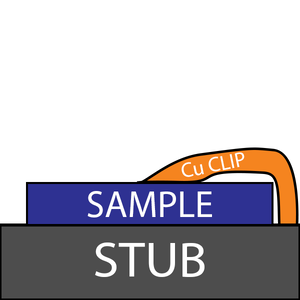
For conductive or nonconductive specimens without carbon tape. Use this method for imaging in the cleanroom.


Cross Section
- Clean, flat edges image best. Cleaved wafers typically have good edges. Ask for cleaving help if you need it. Be aware that the dicing saw tends to create rough edges that are not suitable for image the cross section of thin surface layers.
- Position cross section specimens as close as possible to the flat top surface of a cross section stub for best results.
- A thin strip of copper tape across the surface of a cross sectioned specimen may help improve conductivity.
Theory
Beam Generation
Electron microscopy begins at the top of the column where a source is energized with specific settings, some customizable by the user, to extract a beam of electrons. These electrons are then focused through a series of electromagnetic lenses before being emitted from the end of the pole piece. After a short distance, this beam of electrons interacts with the specimen where it then scatters to produce other signals to be collected by detectors.
Accelerating Voltage
The accelerating voltage, sometimes called the landing voltage, high voltage, or high tension (although these terms have slightly different definitions,) describes the energy supplied to the electron beam at the source. This voltage is the voltage difference that extracts and accelerates electrons away from the source and is typically measured in kilovolts (kV,) but sometimes displayed as keV (kiloelectronvolts, i.e. a kilovolt applied to an electron.) The accelerating voltage determines what features are visible in images, as higher voltages have larger penetration depths while lower voltages reveal more surface detail (although too low of a voltage can reveal irrelevant surface contamination.) Techniques such as EDS tend to require higher voltages to generate the appropriate signals. Too high of a voltage may introduce charging in less conductive specimens, or may hide important thin structures due to a larger penetration depth and interaction volume within the specimen. Theoretically, higher voltages yield sharper probes, and therefore higher resolution.
Emission Current
The emission current determines how many electrons are extracted from the source per unit time. This is measured in microamps (μA.) Typically, the best emission current for imaging is the highest available current to yield the greatest signal from the specimen. However, some cases (especially for nonconductive specimens) may warrant a lower emission current. Not all microscopes allow the user to change the emission current.
Image Formation
Understanding how images are formed helps us understand how to highlight the important aspects of a specimen, interpret images, and know what to do when artifacts or other problems interfere with good image formation. In short:
- the beam rasters (scans) across a specimen surface where
- at each pixel it interacts with a certain volume of the specimen and then
- generates signals that can show topographic detail, material contrast, or specific elements.
Beam-Specimen Interactions
When high energy electrons hit a surface, most of the electrons penetrate some depth into the specimen and interact with the specimen atoms. How far the electrons scatter into the specimen and where they go depends on the type of interaction. However, all of these scattering events happen within some volume known as the interaction volume. The size of this interaction volume is determined by the beam energy (accelerating voltage,) the specimen material, and the type of interaction.
- Higher incident beam energies yield larger interaction volumes within the same material
- Non-conductive materials have larger interaction volumes than conductive materials for a given energy
- Secondary electrons have much less energy than backscattered electrons, so they reveal more surface detail
Because of these factors, images of conductive specimens tend to appear sharper than images of non-conductive specimens captured under the same conditions.
In SEM, three key signals are generated:

- Secondary electrons are produced from the smallest interaction volume closest to the specimen surface, usually a few to tens of nanometers. Secondary electrons show topographic detail, wherein the amount of surface exposed at a given point largely determines how many electrons can reach the detector. This means that edges tend to appear bright, while holes, pits, or cracks appear dark (with a bright edge.) These electrons result from multiple inelastic scattering events and therefore have less energy to escape the specimen surface from deeper within the specimen - hence the small interaction volume.
- Backscattered electrons "bounce" off atoms in a specimen at a rate proportional to the atomic Z, thus revealing material contrast wherein brighter regions contain heavier elements. These electrons result from a single elastic scattering event and therefore have higher energy than secondary electrons, allowing them to escape from a larger interaction volume, typically on the order of a hundred nanometers.
- Characteristic x-rays are produced when an incident beam electron displaces an atomic electron and a higher energy atomic electron falls to the lower energy vacancy. The energy difference between these levels is emitted as a photon with a characteristic wavelength (or energy.) These energies are known for all atoms and dedicated software processes these signals for qualitative and semi-quantitative atomic characterization. Since characteristic x-rays are a release of photons rather than electrons, they are generated and detected from approximately a micron of interaction volume. Check out the EDS page for more information and operating guides on this technique.
Scanning
The electron beam scans (rasters) across a specimen surface point by point, where the signal generated from each point is displayed as a greyscale intensity on a coordinating pixel before moving to the next pixel. The shade of grey is scaled to the number of electrons (intensity) detected.
- Scattered electrons escape specimen surfaces more efficiently at edges or peaks, which results in a higher intensity and brighter appearance known as the edge effect.
- If a specimen is not conductive (or does not have a conductive pathway to ground,) electrons tend to accumulate. This effect is known as charging and distorts images. Charging is exacerbated by slow scan speeds, among other factors.

Random noise collected by the detector results in grainy images. Random noise is by nature random, so increasing the amount of signal generated (and therefore collected) improves this signal to noise ratio (SNR,) thus yielding smoother images and improving the clarity of fine features. The following may increase the SNR:
- Increasing the dwell time, also known as the scan speed: A longer dwell time means more electrons interact with the specimen to produce more signal, while the noise contribution remains constant. Longer dwell times are typically used when capturing images and performing fine alignments, while short dwell times (video rate scan speeds) are great for coarse focus or changing the magnification and stage position.
- Increasing the probe current, also known as the spot size: A larger probe current means there is more current at the specimen surface, and therefore more electrons. This method increases the rate of signal generation, whereas changing the dwell time keeps the rate constant. Increasing the probe current may result in blurry images at high magnifications due to the increased beam diameter at the specimen surface.
- Using frame integration or averaging: Averaging or integrating the signal from multiple frames is similar to increasing the dwell time, but reduces the likelihood of charging since there is time for charge to dissipate between scans. Using more frames is especially effective when the individual frame time is fast and many frames are integrated. In general, to achieve the SNR of a comparable single frame at a slow speed, divide the target dwell time by the dwell time of an individual (stable) frame. Some SEMs have a drift compensation mode available, which compares the position of bright and dark pixels from one frame to the next. Drift compensation may reduce the appearance of drift in features when individual frames contain no visible drift, but the specimen appears to drift from one frame to the next. Drift compensation is not effective for a single frame, nor for multiple slow frames when the drift occurs within a frame.
Signal Collection
Various detectors attract, collect, and process generated signals to convert them into an image. Depending on the type of signal desired, different detectors may be used:
- Secondary electrons are relatively low energy, so a bias is applied to the detector to attract these electrons. It is common for secondary electron detectors to also collect backscattered electrons, however, some detectors have tunable voltage biases to reduce this contribution, if desired.
- Backscattered electrons are relatively high energy and may be collected by reducing the bias of a standard secondary electron detector. Some systems have dedicated backscattered electron detectors which can be mounted directly under the pole piece to take advantage of the difference in takeoff angle between secondary and backscattered electrons, and to reduce the appearance of shadows. Some of these detectors have multiple segments that can be tuned to show shadows or behave similar to a secondary electron detector.
- Characteristic x-rays are very high energy and are collected by a dedicated x-ray detector (an EDS detector) that is often offset to the side and calibrated for a specific working distance. These detectors may need to be installed for each use.

With some detectors, images appear to have shadows. This is most common for detectors that are offset from the beam. Shadows appear in images when signal generated from one part of a specimen is blocked by another, taller part of the specimen. If shadows are obscuring an important portion of a specimen, you may be able to use a different detector if the system has multiple, or rotate the stage. Be aware of the difference between stage and image (or scan) rotation. Stage rotation will change the orientation of the specimen in the chamber, and therefore the position of shadows, while image rotation changes the way the beam scans across the specimen, which does not affect shadows.
Each detector may have a different optimal working distance. Ask staff for assistance or check documentation if you are unsure of the optimal working distance for a given microscope and detector. In some cases, shortening the working distance (carefully) may yield greater signal collection. This is especially true if the detector is mounted above the specimen. However, offset detectors yield diminishing returns when the working distance is too short since the signal is less able to reach the detector.
Charging
Charging presents as different effects depending on the specimen material and topography. In general, charging refers to a buildup or accumulation of electrons on a surface. This buildup tends to occur in nonconductive specimens (material) or specimens without a good conductive pathway connecting the surface to ground via the stub and stage (topography.) Distortions from charging tend to be more apparent at slower scan speeds since the beam dwells longer on a given point. The accumulation of charged particles slows the incident electron beam, which leads to an increased secondary electron emission, thus making portions of the image appear bright. This emission may clear the charge buildup, resulting in a dark region for a frame before returning to bright distortions on the next scan. Charging may appear as drift, high contrast, pulsating or fluctuating brightness, streaks, or blooms. Scroll through the gallery below these descriptions for examples of charging.
- Drift: The sample appears to move continuously in one direction when the stage is stationary. Fast vibrations are not typically due to charging but rather due to an unsecured specimen.
- High contrast: For example, a very bright feature surrounded by a dark ring that does not seem to respond to changing the image contrast.
- Pulsing or fluctuating brightness: The same features may appear dark in one scan and bright in the next, or may actively appear to fluctuate from bright to dark and back, even if scanning at a fast speed. This effect occurs when a specimen is charging then discharging with each electron beam pass.
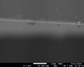
- Streaks: Bright or dark streaks may appear across an image from a point of charging along the row of pixels. This is distinct from streaks seen when a beam is astigmatic since the direction of the streak always follows the scan direction along a row of pixels. Streaks are the result of a delay or residual charge affecting signal collection.
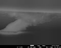
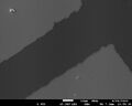
- Bloom: growing and changing "features" on the outer edge of cross section specimens, resulting from the increased electron emission from the surface parallel to the beam path.
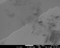
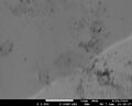
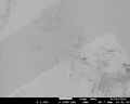
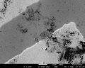
- Charging Examples
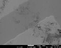
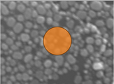
Charging may cause the intensity to pulse between scans.
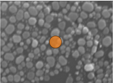
Some areas remain saturated (white) no matter how the brightness and contrast are adjusted.
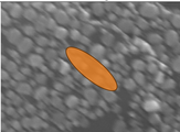
This line displacement suggests the specimen is drifting due to charging. In severe cases, the entire specimen will appear to smear across the image.
Charging creates bright or dark streaks across an image, especially in low vacuum modes or from raised points on a specimen.
On cross section specimens, growing blooms may appear in the vacuum beyond the specimen.
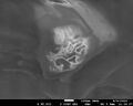
A combination of bloom and streak artifacts on a cross section specimen.
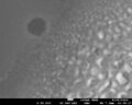
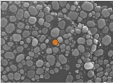
High intensity contrast charging on a particle, which may induce damage to the specimen.


Charging is primarily influenced by sample conductivity, but changing the electron dose (beam energy, current, magnification, and dwell time) may mitigate the effects of charging. Sample conductivity refers not only to the conductivity of the material itself, but also the conductive pathway connecting the specimen to ground and the morphology of the specimen (e.g. clumps of powders or bundles of fibers tend to have poor conductivity if they are too thick.)
In most cases, decreasing the probe current and/or accelerating voltage reduces charging. Some samples will charge regardless of these conditions and must be imaged at fast speeds with frame averaging or integration for noise reduction, or at lower magnifications if possible. In rare cases, a higher accelerating voltage will reduce charging. One such case is for very thin films (10s of nanometers) where the primary beam can penetrate through the nonconductive surface to a conductive substrate below.
The following specimen preparation techniques may reduce charging:
- Sputter coating: the application of a few nanometers of a metal (e.g. iridium) to the surface of a specimen provides a conductive surface for better signal generation and charge dissipation - sometimes the dissipation pathway must be supplemented with copper tape.
- Applying copper tape: this is useful for conductive films on nonconductive substrates, certain sputter coated specimens, etc. The copper tape acts as an adhesive wire to give the electrons an escape route that bypasses the nonconductive substrate. Copper tape works best when pressed firmly against the specimen and close to the area of interest. Stubs or holders with clips function similar to copper tape.
- Ensuring powders and fibers are in a single layer, or as thin a layer as possible to reduce the likelihood of large (to an SEM) clumps or bundles that inhibit the flow of electrons. Be sure to apply only a thin layer (less than you think you need,) and firmly tap off any excess. When imaging, look for the thinnest areas for the best results.
- Using conductive substrates whenever possible: glass slides are notoriously difficult to image in an SEM and require additional practice to find good operating parameters.
If specimen preparation cannot be suitably modified, the specimen may be imaged in a low vacuum SEM. Low vacuum imaging bleeds a small amount of gas or water vapor into the imaging chamber (our Quanta ESEM uses water vapor.) In the presence of the high energy incident electron beam, this gas or vapor will ionize and be drawn to charged areas of a specimen to neutralize the charge.
Some SEMs have multiple available detectors, some of which are more suited for imaging samples prone to charging (e.g. the LEI detector in the 7500F or the LFD in the Quanta). In rare cases where secondary electron imaging is impossible due to charging, imaging with backscattered electrons or altering the bias on the detector may reduce the appearance of charging.
Good Images
Good images in microscopy are not only well aligned, but self-explanatory. A viewer should be able to understand and clearly see the intended features of an image, while the caption provides additional context. Often, an image series helps tell a visual story better than a single image without context. Keep these tips in mind for good images:
- Selecting the appropriate accelerating voltage and currents can reveal or conceal features. Low voltages show surface detail, but too low of a voltage may show undesired surface contamination. High currents may improve the signal to noise ratio, but will blur features at high magnifications. It is best to try a few different settings to understand which combination yields the clearest view of the desired features, while still considering scientific integrity.
- Observe how different voltages change feature clarity
15kV
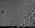
5kV
2kV


- Surface contamination is more visible at low voltages
15kV
2kV


- For high quality images, a well aligned beam is essential. The alignment notes on this page and operating guides provide the tools and theory behind alignment, but practice yields the difference between acceptable alignment and great alignment. An image that is unfocused and astigmatic lacks key details and may distort features in a misleading way. The best advice: practice, but ask for help when needed.
- If the beam is not aligned...
Features stretch when out of focus
Features look blurry even when in focus
But features are clear when aligned


- Image contrast enables the viewer to see differences in topography and material, but both low and high contrast can obscure features. A good greyscale image avoids pure black or pure white pixels while using as much of the available greyscale spectrum. Images may appear noisier with good contrast, which should be compensated for by scanning for a longer time or integrating multiple frames to collect more signal. When in doubt, most systems allow the user to see the greyscale histogram and ensure that the spread is reasonable without saturating any important features.
- Note: capturing images in 16-bit format (available on most SEMs in the NCF) with reduced contrast allows for more postprocessing in programs like ImageJ or Photoshop without losing image quality or integrity.
- Contrast and brightness affect feature clarity
Low contrast and high brightness wash out an image
Features are more clear and no areas are saturated
High contrast and low brightness obscure low and high signal features


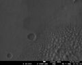
- Images should include visual context such as nearby features or devices whenever possible. Capturing images at appropriate magnifications facilitates comprehension. Serial magnifications should be in reasonable increments to avoid confusion. In general, a 2-5X increase in magnification (e.g. from 50X to 250X) maintains enough visual context for easy comprehension.
- When capturing serial magnifications, it is often beneficial to start at the highest magnification then zoom out in steps so the key field of view remains centered. However, for specimens prone to charging or beam damage, it may be better to start at the lowest magnification then zoom in to avoid the presence of raster boxes within lower magnification images - just ensure that the features of interest are easy to follow from one magnification to the next.
- Visual context helps a reader comprehend high magnification images
high magnification images are great for showing small details
but low magnification images contextualize features
Alignment
There are three key alignments in SEM: focus, aperture position, and astigmatism correction. After performing an initial alignment at a sufficiently high magnification, the system should remain well aligned, needing only small adjustments when moving from one sample to another, changing working distances, or zooming in. The beam alignment should be checked whenever beam settings are changed, including the accelerating voltage and probe current.
Focus
Focusing means moving the smallest cross section of the electron probe to the specimen surface to produce the sharpest image.
- The plane normal to the beam containing this cross section is called the focal plane.
- The position of the focal plane relative to the pole piece (where the beam is emitted from the column) is defined as the working distance.
- When a specimen is in focus, the working distance describes where the specimen surface is, relative to the pole piece.
- In some systems, the working distance can be linked to the stage height.
- In general, the position of the specimen according to any stage height indicators or displays should be considered an estimate. The real position of the specimen is defined by the working distance when the specimen is in focus.

When an image is out of focus, it appears blurry because the probe cross section is larger than the features being imaged or because the probe is larger than the pixels in the image.
- At low magnifications, a specimen will appear in focus for a large range of working distances due to the small size of the probe relative to the pixel and/or feature size.
- If an image is still blurry when in focus, or if it is difficult to focus because the image appears sharper at two different working distances (with a blurry image in between,) then the beam is likely astigmatic and the stigmators need to be tuned to reshape the beam.
- On specimens with large height variations or when tilting to a high degree, a portion of the image may appear blurry while other portions are in focus. This is due to the limited depth of field. Some SEMs have a control that enables the user to tune the depth of field.
Apertures
Only a small portion of the beam generated at the source is selected for final imaging by an aperture, which may need to be centered in the beam path. If this aperture is not centered, then the beam is not normal to the imaging plane (which results in other alignment distortions, especially when working at high magnifications, imaging highly topographic specimens, or using long working distances,) and the beam may not be as bright as possible.
To ensure that the brightest, most central, on-axis portion of the beam is selected, the user must observe whether the image shifts when the focal plane shifts, which indicates that the aperture is not centered. Most SEMs will "wobble" the beam automatically. This function has different names on different systems, including lens align, wobb, aperture align, etc. Ask microscopy staff if you are uncertain.

The alignment itself is completed with a pair of X and Y axis controls (either physical knobs or on a computer interface) to move the aperture inside the SEM. At low magnifications (typically below 10kX) the image may appear to rotate when the wobbler is engaged. This is normal. It should rotate around the center, but may be easier to align at a higher magnification where the rotating effect is visibly minimized.
Zoom in to a higher magnification than is desired for final imaging for this step and pay attention to how the image behaves at the center of the screen. Most systems have a crosshair or alignment marker available to designate the center of the image.
Stigmators
An ideal electron beam is circular in cross section regardless of focus. This means the features blur uniformly in all directions when out of focus and achieve the sharpest image when in focus. If the cross section is not circular when out of focus, the beam is considered astigmatic and will be blurry even when in focus. This is because the electrons are not focusing to the same point, so the probe is larger than it can be.
In focus with stigmators aligned
Out of focus with stigmators aligned
In focus with astigmatism


Astigmatic beams cause the image to stretch when out of focus, and this stretching effect is directionally perpendicular to itself on either side of focus. Consequently, astigmatism can be identified by moving the focal plane to either side of focus and observing whether the image appears distorted in opposite directions. Ideally, the image should appear the same on either side of focus.
Out of focus with astigmatism
In focus with astigmatism
Other side of focus with astigmatism


When changing the focus, the following image behavior indicates astigmatism is present:

The stigmators knobs on an SEM enable the user to control and reshape the beam with a set of magnetic fields. These are labeled X and Y, but do not correspond to the X and Y directions. They instead control (typically) two sets of perpendicular axes, offset by about 45 degrees to one another.
If astigmatism is identified, it can be corrected by first going to focus (directly between the two perpendicularly stretching directions) then adjusting one stigmator at a time until the image appears sharpest. Astigmatism may also be corrected when out of focus by observing how the image distortion changes with each knob and finding a "midpoint" for each axis before returning to focus. Ask staff for a demonstration if you are struggling to align the stigmators.
Out of focus with astigmatism
In focus with astigmatism
Other side of focus with astigmatism
If both stigmators are out of alignment, adjusting one when out of focus may look like this:

An example of a stigmator alignment procedure:

Troubleshooting
Achieving a sharp image in SEM takes practice is often hindered by something other than focus alone. It is important to ask the right questions when troubleshooting to find the best solution and improve image quality:
Are the beam settings appropriate for this sample?
Every sample interacts with the electron beam differently depending on material, geometry, and preparation. Beam voltage and spot size allow users to tune some of these interactions. Consider:
- Which is more important: thin surface structures or fine details?
- Lower voltages show thin structures better due to the smaller interaction volume, which means a smaller proportion of signal comes from the bulk or substrate of the specimen.
- Is the sample charging?
- Lower currents tend to reduce charging.
- Typically, lowering the voltage also reduces charging, but there are some exceptions (e.g. thin nonconductive films on conductive substrates, operation in low vacuum mode.)
There will always be a balance between beam energy, specimen damage, charging, and image quality. Try changing one setting at a time in either direction (higher/lower, larger/smaller) and observe how the sample responds.
Is the beam aligned?
Remember these three components of alignment:
- Focus: The focal plane should be on the sample surface, which yields the sharpest image.
- If focus is difficult to find, it may mean the stigmators are not aligned. If direction stretching or smearing of features is observed, look for a second, perpendicular direction at a different focal plane. The true focal plane lies directly between these two positions.
- Aperture/Lens alignment: The aperture should be positioned so the specimen image pulses in and out of focus without shifting in X or Y when the wobbler is turned on.
- Rotation of the image is normal below 10,000X. Zoom in past this magnification for easier alignment, and pay attention to how the image moves at the center of the image.
- Stigmators: The specimen image should look about the same on either side of focus, rather than appearing stretched in perpendicular directions on either side of focus. Find the focal plane, then adjust the X and Y stigmators one at a time until the image is sharpest.
If you are having trouble focusing, the number one reason is that the beam is astigmatic.
- Zoom in (or out) to at least 10,000X and navigate to an area with numerous small features. These do not need to be important features. Edges, scractes, or sample holder surfaces are fine. Ideally look for an area with small round or random features.
- Adjust the focus and look for any stretching. If the image smears in two different directions depending on the focus, place the focus in the middle of these two working distances.
- One at a time, adjust the stigmators. Look for the sharpest image. Check your work by moving the focus up and down and look for either stretching (still astigmatic) or the sharpest images (your focal plane when aligned.)
Is the right signal reaching the detector?
SEMs collect signal with a single-point detector, not an array like the detector in a camera. It is important to remember that the following impact image quality and feature clarity:
- Beam-Specimen Interactions, or how the signal comes from the specimen.
- High voltages may obscure thin surface features, just as large probe currents can obscure fine details.
- How signal reaches the detector, or the position of the detector relative to the specimen. Tilted and highly topographic specimens may cast shadows where signal is blocked. Try rotating the stage or using a different detector.
- The sample may need to be moved to a shorter working distance to improve contrast. Be careful to watch how the stage moves in the chamberscope to avoid collisions. Be aware of stage limits and ask for help if needed.
- How images are formed, including scanning rates and image size or pixel resolution.
- Slowing the scan speed or integrating multiple frames of a faster speed can improve the signal-to-noise ratio (SNR.)
Is there a better way to prepare the sample?
Sample preparation can help or impede signal generation. Generally speaking, well prepared samples produce better images. Consider:
- How the sample itself is prepared. Is it clean? Vacuum compatible? Are there other contaminants/reactants/residues? Are the features easy to find or somehow marked?
- How the sample is secured to the stub. Is there a conductive pathway? Is there too much specimen? Will it vibrate?
With some exceptions for low-vacuum SEM, ensure there is a conductive pathway between the specimen surface and the stub. This may mean coating, adding copper tape or a conductive clip, pressing specimens better to carbon tape, using a conductive substrate, or ensuring powders or fibers are adhered in as thin a layer as possible. Remember: what may seem small to us, is still large to the SEM. Failure to secure or ground specimens may result in charging or drift that negatively impacts image quality.
Remember that SEM is a skill and every sample is different - take time to practice and observe how images change in response to beam settings and alignments.