Difference between revisions of "Lesker PVD75 E-beam Evaporator"
Jump to navigation
Jump to search
(update to NEMO) |
|||
| (9 intermediate revisions by 3 users not shown) | |||
| Line 1: | Line 1: | ||
| − | [[Category:Deposition]] | + | [[Category:Deposition]][[Category:Physical Vapor Deposition]][[Category:Evaporation]][[Category:Equipment]] |
{{EquipmentInfo | {{EquipmentInfo | ||
| Line 23: | Line 23: | ||
The tool contains the following materials: | The tool contains the following materials: | ||
| − | * Au - Gold | + | * [[Au (gold) | Au - Gold]] |
* Cr - Chromium | * Cr - Chromium | ||
* Pd - Palladium | * Pd - Palladium | ||
| − | * Ti - Titanium | + | * [[Ti (titanium) | Ti - Titanium]] |
Deposition is limited to thin-film thicknesses of ~100 nm. | Deposition is limited to thin-film thicknesses of ~100 nm. | ||
| Line 36: | Line 36: | ||
===== SOPs & Troubleshooting ===== | ===== SOPs & Troubleshooting ===== | ||
| − | Link: [https://repository.upenn.edu/scn_sop/23/ | + | Link: [https://repository.upenn.edu/scn_sop/23/ SOP] |
| + | |||
| + | <pdf height="800">File:PVD04 SOP v07.pdf</pdf> | ||
Latest revision as of 08:54, 4 September 2025
 |
|
| Tool Name | Lesker PVD75 E-Beam/Thermal Evaporator |
|---|---|
| Instrument Type | Physical vapor deposition |
| Staff Manager | David Barth |
| Lab Location | Bay 2 |
| Tool Manufacturer | Kurt J. Lesker |
| Tool Model | PVD75 |
| NEMO Designation | PVD-04 |
| Nearest Phone | 215-898-9748 |
| SOP Link | SOP |
Description
The tool
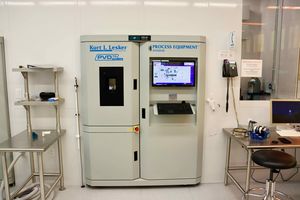
The Kurt J. Lesker PVD75 E-beam Evaporator is an electron-beam (e-beam) evaporation tool. The tool is a fully automated system for depositing Ti, Cr, Au, and/or Pd. The tool also comes with a load-lock, allowing for fast and easy transfer of samples in and out of the system. While less flexible than the PVD-02 deposition system in terms of available materials, the PVD-04 is a much faster tool.
Available materials
The tool contains the following materials:
- Au - Gold
- Cr - Chromium
- Pd - Palladium
- Ti - Titanium
Deposition is limited to thin-film thicknesses of ~100 nm.
Resources
Training video
Link: PVD-4 Training Video
SOPs & Troubleshooting
Link: SOP