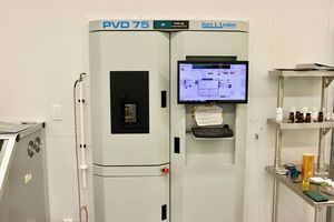
Lesker PVD75 E-Beam/Thermal Evaporator
 |
|
| Tool Name | Lesker PVD75 E-Beam/Thermal Evaporator |
|---|---|
| Instrument Type | Deposition |
| Staff Manager | David Barth |
| Lab Location | Bay 2 |
| Tool Manufacturer | Kurt J. Lesker |
| Tool Model | PVD75 |
| NEMO Designation | PVD-02 |
| Lab Phone | 215-898-9748 |
| SOP Link | SOP |
Description
The Kurt J. Lesker PVD 75 thin film deposition system is equipped for electron-beam (4 pockets) and thermal evaporation (2 sources). The evaporator is used to deposit many metals and some semiconductor and dielectric materials. E-beam is the preferred evaporation technique for the high melting point materials. Evaporation provides directionality in depositions, which is beneficial when doing liftoff metallization (as opposed to conformal coating with sputtering deposition). Crystal oscillators are used to monitor deposition rates and thickness.
The system can accommodate pieces through wafers up to 150 mm in diameter and is configured with platen rotation and a cooling stage.
Deposition Sources
A wide variety of materials are used in this tool. Certain materials with high vapor pressure or a high likelihood to contaminate other processes (such as indium) are not allowed. While some common materials are provided by the QNF, users are responsible for keeping and maintaining their own melts. Some of the more commonly used materials are listed below.
Metals and metalloids
- Ag - Silver
- Al - Aluminum
- Au - Gold
- Cr - Chromium
- Cu - Copper
- Ge - Germanium
- Pt - Platinum
- Ti - Titanium
Oxides
- SiO2 - Silica
- Al2O3 - Alumina
PROHIBITED MATERIALS
- In - Indium (must be deposited in PVD-01)
- InAs - Indium arsenide
- InSb - Indium antimonide
- Pb - Lead
- Sn - Tin (must be deposited in PVD-01)