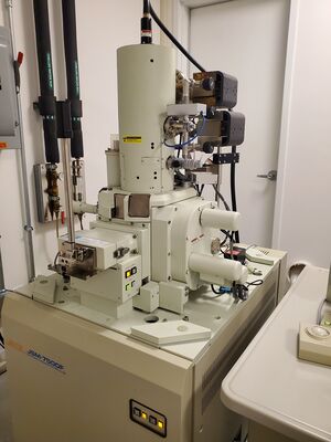
JEOL 7500F HRSEM
 |
|
| Tool Name | 7500F |
|---|---|
| Instrument Type | SEM |
| Staff Manager | Jamie Ford, Nicole Bohn |
| Lab Location | Bay 6 |
| Tool Manufacturer | JEOL, Inc. |
| Tool Model | 7500F HRSEM |
| NEMO Designation | JEOL 7500F HRSEM |
| Nearest Phone | XXXXX |
| SOP Link | 7500F Reference Guide |
Description
The JEOL 7500F Scanning Electron Microscope provides ultrahigh resolution of 0.8 nm at 30 kV and 1 nm at 1 kV. This SEM operates in high vacuum and is best suited for conductive specimens, but its low voltage resolution enables some nonconductive imaging. The 7500F is in the NCF Annex, located in Bay 6 of the Quattrone Nanofabrication Facility. Access to the cleanroom is required for access to the microscope. This microscope is especially useful for mid-process characterization
Detectors
Secondary and backscattered electron detectors allow for imaging of sample surfaces, whereas a scanning-transmission electron detector shows the internal structure of materials. Through a stage biasing system, referred to as “gentle-beam” mode, the electron beam interacting with the sample may be reduced to a fraction of the accelerating voltage of the gun, allowing for the imaging of soft or insulating samples without the need for carbon or metal coating. An EDAX Energy Dispersive x-ray spectrometer (EDS) is available for chemical characterization via spectra or element maps.
Sample Holders
Compatible sample holders are required when loading specimens into the 7500F, and the appropriate holder must be selected after loading the specimen onto the stage. A guide for holder icon selection is available on our reference website
EDS with APEX
APEX by EDAX is installed on the companion computer for EDS data collection and analysis. A guide for this program is available on our reference website.