Difference between revisions of "EVG 620 Wafer Bond Aligner"
Jump to navigation
Jump to search
m (Protected "EVG 620 Wafer Bond Aligner" ([Edit=Allow only administrators] (indefinite) [Move=Allow only administrators] (indefinite)) [cascading]) |
m |
||
| (3 intermediate revisions by 2 users not shown) | |||
| Line 1: | Line 1: | ||
| − | [[Category: | + | [[Category:Backend & Packaging]][[Category:Equipment]] |
{{EquipmentInfo | {{EquipmentInfo | ||
| Line 7: | Line 7: | ||
| imagecaption = | | imagecaption = | ||
| Instrument_Type = Back End | | Instrument_Type = Back End | ||
| − | | Staff_Manager = Eric Johnston | + | | Staff_Manager = [[Eric Johnston | Eric Johnston]] |
| − | | Lab_Location = Bay | + | | Lab_Location = Bay 4 |
| Tool_Manufacturer = EV Group | | Tool_Manufacturer = EV Group | ||
| Tool_Model = 620 Aligner | | Tool_Model = 620 Aligner | ||
| − | | | + | | NEMO_Designation = BE-02 |
| Lab_Phone = XXXXX | | Lab_Phone = XXXXX | ||
| SOP Link = [https://www.seas.upenn.edu/~nanosop/Wafer_Bond_Aligner_SOP.htm SOP] | | SOP Link = [https://www.seas.upenn.edu/~nanosop/Wafer_Bond_Aligner_SOP.htm SOP] | ||
Latest revision as of 12:38, 28 July 2025
 |
|
| Tool Name | EVG 620 Wafer Bond Aligner |
|---|---|
| Instrument Type | Back End |
| Staff Manager | Eric Johnston |
| Lab Location | Bay 4 |
| Tool Manufacturer | EV Group |
| Tool Model | 620 Aligner |
| NEMO Designation | BE-02 |
| Nearest Phone | XXXXX |
| SOP Link | SOP |
Description
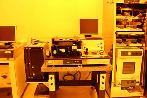
Known for its high level of automation and reliability, the EVG620 Bond Alignment System is designed for wafer-to-wafer alignment up to 150 mm wafer sizes. The EV Group´s bond alignment systems offer highest precision, flexibility, ease of use and modular upgrade capability and have been qualified in numerous high throughput production environments. The precision of EVG´s bond alignment system accommodates most demanding alignment processes in MEMS production and in emerging fields like 3D integration applications.
Applications
- Aligning 4" wafers for bonding in the EVG 620
- Maximum stack height: 4.5 mm
- Range of alignment: X, Y ± 5.0 mm
- Alignment accuracy:
- 0.5 um for glass/silicon
- 1.0 um for silicon/silicon
- Contact force: 1-40 N