Difference between revisions of "SPTS Si DRIE"
m (Protected "SPTS Si DRIE" ([Edit=Allow only administrators] (indefinite) [Move=Allow only administrators] (indefinite)) [cascading]) |
m |
||
| (17 intermediate revisions by 3 users not shown) | |||
| Line 1: | Line 1: | ||
| − | [[Category:Etch]] | + | [[Category:Etch]][[Category:Plasma Etch]][[Category:Equipment]] |
{{EquipmentInfo | {{EquipmentInfo | ||
| Line 7: | Line 7: | ||
| imagecaption = | | imagecaption = | ||
| Instrument_Type = Etch | | Instrument_Type = Etch | ||
| − | | Staff_Manager = | + | | Staff_Manager = [[Lucas Barreto | Lucas Barreto]] |
| Lab_Location = Bay 2 | | Lab_Location = Bay 2 | ||
| Tool_Manufacturer = SPTS | | Tool_Manufacturer = SPTS | ||
| Tool_Model = Rapier | | Tool_Model = Rapier | ||
| − | | | + | | NEMO_Designation = DE-03 |
| − | | Lab_Phone = | + | | Lab_Phone = 215-898-9748 |
| SOP Link = [https://repository.upenn.edu/scn_sop/11 SOP] | | SOP Link = [https://repository.upenn.edu/scn_sop/11 SOP] | ||
}} | }} | ||
| Line 27: | Line 27: | ||
* Deep etching of Si | * Deep etching of Si | ||
| + | ===== Etch masks allowed (and selectivity values) ===== | ||
| + | * Resist with selectivity of ~ 20:1 (resist:Si) for features with CD of ~ few microns and depths of up to ~ 200-300 um. | ||
| + | * SiO2, SiNx, Al2O3, AlN with extremely high selectivity to AlN and Al2O3 and selectivity of ~ 100:1 for SiO2. | ||
| + | |||
| + | - No metal is allowed in the chamber! | ||
| + | |||
| + | ===== Post etch sample cleaning procedure ===== | ||
| + | We recommend an O<sub>2</sub> plasma in a barrel asher for removal of residue of the passivation layer as well as remainder of resist mask. | ||
| + | |||
| + | The standard cleaning recipe is a 300 Watt O<sub>2</sub> plasma for 1 hour, with 100 sccm O<sub>2</sub> flow - see [[Anatech SCE-108 Barrel Asher |DE-02]] tool page. | ||
== Resources == | == Resources == | ||
| − | [https://repository.upenn.edu/ | + | [https://repository.upenn.edu/handle/20.500.14332/45848 SPTS Etch Recipe Characterization] |
[https://www.youtube.com/watch?v=UmRFj_2kdJ8 Training Part 1, Introduction & Wafer Cleaning] | [https://www.youtube.com/watch?v=UmRFj_2kdJ8 Training Part 1, Introduction & Wafer Cleaning] | ||
Latest revision as of 15:52, 25 July 2025
 |
|
| Tool Name | SPTS Si DRIE |
|---|---|
| Instrument Type | Etch |
| Staff Manager | Lucas Barreto |
| Lab Location | Bay 2 |
| Tool Manufacturer | SPTS |
| Tool Model | Rapier |
| NEMO Designation | DE-03 |
| Nearest Phone | 215-898-9748 |
| SOP Link | SOP |
Description
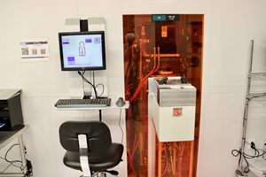
SPTS Rapier is an anisotropic dry etch tool. The tool uses Bosch Process to etch silicon with high selectivity and nearly vertical sidewalls. Bosch process consists of two steps: 1) Deposition of a passivation layer, using C4F8 gas. This passivation layer is a polymer that protects the sidewalls from being etched. 2) A nearly vertical plasma etch step using SF6. A bias is applied in the chamber that forces the ions to attack the surface vertically and etch through the passivation layer at the bottom of the trench, exposing the silicon underneath. That Si is then etched within the same step. The passivation layer is also deposited inside the chamber and the etch results in a layer of deposited polymer inside the chamber walls which makes it critical to run a cleaning recipe at the end of each etch run.
Shorter cycle times result in smoother sidewalls while longer cycle times achieve higher etch rate. The tool in QNF is connected to Ar, O2,N2, C4F8, and SF6 gases.
Applications
- Deep etching of Si
Etch masks allowed (and selectivity values)
- Resist with selectivity of ~ 20:1 (resist:Si) for features with CD of ~ few microns and depths of up to ~ 200-300 um.
- SiO2, SiNx, Al2O3, AlN with extremely high selectivity to AlN and Al2O3 and selectivity of ~ 100:1 for SiO2.
- No metal is allowed in the chamber!
Post etch sample cleaning procedure
We recommend an O2 plasma in a barrel asher for removal of residue of the passivation layer as well as remainder of resist mask.
The standard cleaning recipe is a 300 Watt O2 plasma for 1 hour, with 100 sccm O2 flow - see DE-02 tool page.
Resources
SPTS Etch Recipe Characterization
Training Part 1, Introduction & Wafer Cleaning
Training Part 2, Operating The Tool