Difference between revisions of "PECVD SiNx via CHF3 + O2"
| (2 intermediate revisions by the same user not shown) | |||
| Line 17: | Line 17: | ||
== Materials == | == Materials == | ||
| − | * Microchem S1818 Photoresist | + | * [[Resists at QNF|Microchem S1818 Photoresist]] |
| − | * Microchem MF-319 Developer | + | * [[Developers at QNF|Microchem MF-319 Developer]] |
* 4 inch Silicon Wafers | * 4 inch Silicon Wafers | ||
| Line 36: | Line 36: | ||
=== Expose === | === Expose === | ||
| − | 1. Use the photomask to expose the wafer at 150 mJ/cm2 | + | 1. Use the photomask to expose the wafer at 150 mJ/cm2 |
1. Dispense approximately 150 milliliters of MF-319 developer into a six inch cylindrical container. | 1. Dispense approximately 150 milliliters of MF-319 developer into a six inch cylindrical container. | ||
| Line 54: | Line 54: | ||
* RF Power: 150 W | * RF Power: 150 W | ||
* Capacitor starting points: Capacitor #1: 60 %, Capacitor #2: 80 % | * Capacitor starting points: Capacitor #1: 60 %, Capacitor #2: 80 % | ||
| − | |||
== Results == | == Results == | ||
Latest revision as of 15:47, 16 September 2024
Process description
This process is performed to measure the etch rate of PECVD SiNx using an Oxford 80 plus RIE tool. Lithography equipment and material used in this study can be substituted by others that would result in a similar pattern.
recipe name on the tool: 00_Staff_CHF3/O2
Equipment
Units
- Gas flow rate: standard cubic centimeters per minute (sccm)
- Pressure: milliTorr (mT)
- Temperature: degrees Celsius (C)
- High frequency (RF) power: Watts (W)
Materials
- Microchem S1818 Photoresist
- Microchem MF-319 Developer
- 4 inch Silicon Wafers
Protocol
Coat
1. Mount wafer and ensure that it is centered.
2. Deposit 7 milliliters of S1818 photoresist in the center of the wafer.
3. Spin on photoresist at 4500 RPM for 60 Seconds.
Soft Bake
1. Bake wafer at 115 °C for 60 seconds.
Expose
1. Use the photomask to expose the wafer at 150 mJ/cm2
1. Dispense approximately 150 milliliters of MF-319 developer into a six inch cylindrical container.
2. Fully submerge the exposed wafer.
3. Agitate and develop the wafer for 60 seconds.
Etch
1. Pump to 5e-04 Torr, “Pump to Pressure” checked.
2. Etch Step (etch recipe done via recipe named: 00_Staff_CHF3/O2 on the QNF tool)
- Trifluoromethane (CHF3) flow rate: 100 sccm Oxygen (O2) flow rate: 4 sccm
- Pressure: 50 mT
- RF Power: 150 W
- Capacitor starting points: Capacitor #1: 60 %, Capacitor #2: 80 %
Results
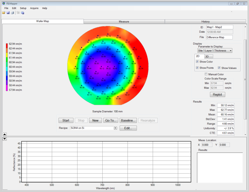
etch rate ~ 60 nm/min - measured on a 4" wafer on July 29th, 2024
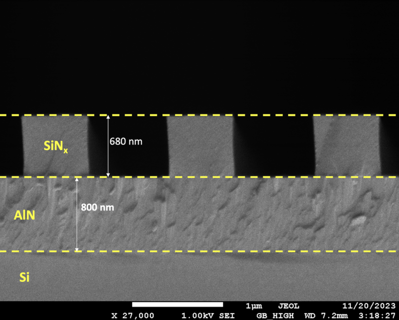
Side SEM of a two step SiNx etch, totaling ~ 12 minutes

