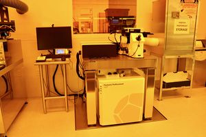
Nanoscribe Photonic Professional GT
 |
|
| Tool Name | Nanoscribe Photonic Professional GT+ |
|---|---|
| Instrument Type | Lithography |
| Staff Manager | Ana Cohen |
| Lab Location | Bay 6 |
| Tool Manufacturer | Nanoscribe |
| Tool Model | Photonic Professional GT+ |
| NEMO Designation | LW-02 |
| Nearest Phone | XXXXX |
| SOP Link | SOP |
Description
The Nanoscribe Photonic Professional enables the fabrication of true 3D structures in the microscale via two-photon polymerization using a 780nm laser with ~100fs pulse, 80MHz repetition rate. This system allows for cutting-edge research and rapid prototyping in microfluidics, MEMS, microoptics, nanostructures and more.
Upgraded to GT+ in Dec 2024! Includes new housing with easier objective loading with 10x objective capability and greater print height (previously 3mm)
Tool Features
- Laser Power: 50-150mW
- Print Height: Up to 8mm
- Lateral resolution ~ 200 nm
- Vertical resolution ~ 300 nm
- Piezo scanning range: 300 x 300 x 300 μm3
- Stage scanning range: 100 x 100 mm2
Available Print Sets
| Objective | Voxel size (width) | Print field radius | Print time (per mm3) | Compatible Resins | Compatible Substrates |
|---|---|---|---|---|---|
| 63x | ~0.2 μm | 100 μm | ~2.5 hr | IP-Dip, IP-PDMS, IP-L | Fused Silica Glass, ITO/Soda Lime Glass, Silicon |
| 25x | ~0.6 μm | 200 μm | ~1.25 hr | IP-S, IP-PDMS, IP-L, IP-Visio | ITO/Soda Lime Glass, Silicon |
| 10x | ~1.2 μm | 500 μm | ~10 min | IP-Q, IP-PDMS | Silicon |
Voxel = the smallest printable 3D volume, the 3D analogue of a 2D pixel. Single voxels are not mechanically stable. Multiple neighboring voxels/lines are recommended for stable structures.
Print field = the circular region an objective could write without moving the stage. Structures that exceed the print field of the objective must be split into blocks in Describe.
Print time = how long to take to print a 10 μm cube (1 mm3). The print times for the 25x and 10x are calculated for shell recipes. Solid recipes would take longer to print the same volume.
Allowed Materials
Other materials must have tool owner approval before use in this system!
Substrates
4" Wafers
- Silicon, 500μm thickness
25mm x 25mm
- Silicon, 700μm or 500μm thickness
- ITO-coated Soda Lime Glass - only if provided by Nanoscribe
- Fused Silica Glass - only if provided by Nanoscribe
All substrates are available in the QNF Stockroom
Resists
- IP-Dip
- IP-S
- IP-Q
- IP-PDMS
- IP-L
- IP-Visio
All resists are currently available as a QNF supplied materials and do not require separate purchase. More information about these resists can be found here
Training Protocol
1. Remote session on EBL-02 for the Describe conversion software, using your structure (90min)
2. In-person session on LW-02 (120min)
3. Qualification session on LW-02, where you run the tool with minimal input (~60min) -- must be done after previous two sessions are completed, cannot be done the same day as the in-person training
All should be requested through NEMO.