File:DWL schematic.PNG
Jump to navigation
Jump to search
Size of this preview: 606 × 599 pixels. Other resolutions: 243 × 240 pixels | 888 × 878 pixels.
Original file (888 × 878 pixels, file size: 196 KB, MIME type: image/png)
Summary
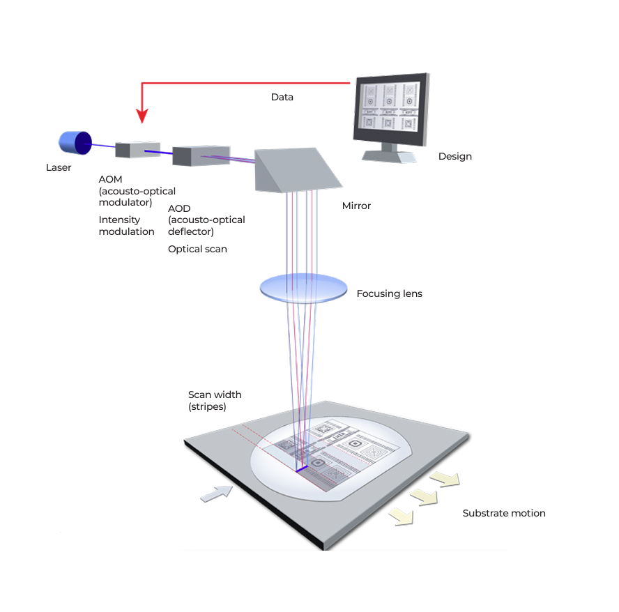
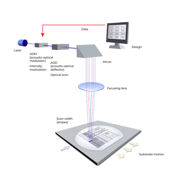
Schematic of pattern exposure with the DWL66+ Source -- TheLithographer.com, Surface Issue, May 2025 [1]
File history
Click on a date/time to view the file as it appeared at that time.
| Date/Time | Thumbnail | Dimensions | User | Comment | |
|---|---|---|---|---|---|
| current | 15:12, 24 July 2025 | | 888 × 878 (196 KB) | Coana (talk | contribs) | Schematic of pattern exposure with the DWL66+ Source -- TheLithographer.com, Surface Issue, May 2025 [https://heidelberg-instruments.com/wp-content/uploads/2025/05/The-Lithographer-Surface-Issue.pdf] |
You cannot overwrite this file.
File usage
The following page uses this file: