Difference between revisions of "Heidelberg DWL 66+ Laser Writer"
| (19 intermediate revisions by the same user not shown) | |||
| Line 1: | Line 1: | ||
| − | [[Category:Lithography]] | + | [[Category:Lithography]][[Category:Photolithography]][[Category:Equipment]] |
{{EquipmentInfo | {{EquipmentInfo | ||
| name = Heidelberg DWL 66+ Laser Writer | | name = Heidelberg DWL 66+ Laser Writer | ||
| Tool_Name = Heidelberg DWL 66+ Laser Writer | | Tool_Name = Heidelberg DWL 66+ Laser Writer | ||
| − | | image = [[Image:LW-01.jpeg| | + | | image = [[Image:LW-01.jpeg|250px]] |
| imagecaption = | | imagecaption = | ||
| Instrument_Type = Lithography | | Instrument_Type = Lithography | ||
| Line 17: | Line 17: | ||
== Description == | == Description == | ||
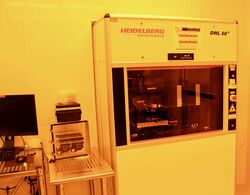
| − | The fully automated DWL 66+ laser writing system | + | The fully automated DWL 66+ laser writing system has both binary (2D) and grayscale (2.5D) exposure capability. |
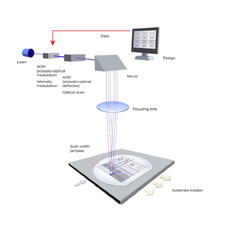
| + | [[File: DWL schematic.PNG|thumb|right|upright=0.75|Schematic of pattern exposure with the DWL66+, [https://heidelberg-instruments.com/wp-content/uploads/2025/05/The-Lithographer-Surface-Issue.pdf TheLithographer.com, Surface Issue, May 2025] ]] | ||
| + | The pattern is broken into vertical stripes of ~500px with preset overlap. To write each stripe, the tool modulates and deflects the laser beam based on the provided pattern data while the stage moves along Y. This process repeats along the X direction until the pattern is complete. | ||
| − | + | == Allowed Materials == | |
| − | + | Substrates | |
| − | |||
| − | |||
| − | |||
| − | |||
| − | |||
| − | |||
| − | |||
| − | |||
* Mask Plates -- available in the [https://nemo.nano.upenn.edu/stockroom/ QNF Stockroom] pre-coated with AZ1500 and IP3500 | * Mask Plates -- available in the [https://nemo.nano.upenn.edu/stockroom/ QNF Stockroom] pre-coated with AZ1500 and IP3500 | ||
| − | * Resists -- must be compatible with h-line exposure | + | * 4" wafers |
| − | + | * Pieceparts > 20mm x 20mm ''(Starting Aug 2025, DMO system is recommended for small piece part direct write) | |
| − | + | Resists -- must be compatible with h-line/ 405nm exposure ''(Laser exchanged in June 2023. Previous documentation may include 365nm capability.)'' | |
| − | + | * [[Resists_at_QNF#QNF_Supplied_Standard_Photoresists | S1800 series]] | |
| + | * [[Resists_at_QNF#Miscellaneous | KL5300 series]] | ||
| + | * [[Resists_at_QNF#Other_Resists | LOR]] | ||
== Processes == | == Processes == | ||
| − | + | === Writehead Selection === | |
| − | + | <u><small>'''NOTE</u>:'''</small>'' Pneumatic mode not currently recommended for dry etch and features under 10x listed minimum feature size due to focus issues -- working with Heidelberg service to address. </br> Last confirmed November 2025.'' | |
{| class="wikitable" style="vertical-align:bottom;" | {| class="wikitable" style="vertical-align:bottom;" | ||
|- | |- | ||
! Write Head | ! Write Head | ||
| − | ! Focus | + | ! Optical Focus |
| − | ! | + | ! Pneumatic Focus |
| − | ! | + | ! Minimum Feature Size |
|- | |- | ||
| 10mm | | 10mm | ||
| + | | -60 | ||
| -100 | | -100 | ||
| − | | | + | | 2um |
| − | |||
| − | |||
| − | |||
| − | |||
| − | |||
| − | |||
|- | |- | ||
| 2mm | | 2mm | ||
| + | | +50 | ||
| -100 | | -100 | ||
| − | | | + | | 600nm |
| − | |||
| − | |||
| − | |||
| − | |||
| − | |||
| − | |||
|- | |- | ||
| 40mm | | 40mm | ||
| + | | N/A | ||
| -100 | | -100 | ||
| − | | | + | | 10um |
| − | |||
|} | |} | ||
| − | + | ===Exposure Parameters=== | |
| + | =====Mask Plates===== | ||
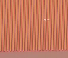
| + | [[File: 10mm n70opt 4.jpg|thumb|right|upright=0.75| 2um lines on AZ1500 using 10mm with optical focus (June 2025)]] | ||
| + | ''530nm resist thickness on chrome-coated soda lime, purchased from TELIC. Development in TMAH 0.26N for 60s. Values last confirmed July 2025.'' | ||
| + | ======AZ1500====== | ||
| + | ''Lower contrast resist - the default option for most applications'' | ||
{| class="wikitable" style="vertical-align:bottom;" | {| class="wikitable" style="vertical-align:bottom;" | ||
|- | |- | ||
| − | |||
! Write Head | ! Write Head | ||
! Filter(s) | ! Filter(s) | ||
! Laser Power | ! Laser Power | ||
! Intensity | ! Intensity | ||
| − | |||
|- | |- | ||
| − | |||
| 10mm | | 10mm | ||
| 50% | | 50% | ||
| 60 mW | | 60 mW | ||
| 90 | | 90 | ||
| − | |||
|- | |- | ||
| − | | IP3500 | + | | 2mm |
| + | | 12.5% + 25% | ||
| + | | 60 mW | ||
| + | | 80 | ||
| + | |- | ||
| + | | 40mm | ||
| + | | NONE | ||
| + | | 220 mW | ||
| + | | 60 | ||
| + | |} | ||
| + | ======IP3500====== | ||
| + | ''Higher contrast resist - produces better corners and small pitch gratings'' | ||
| + | {| class="wikitable" style="vertical-align:bottom;" | ||
| + | |- | ||
| + | ! Write Head | ||
| + | ! Filter(s) | ||
| + | ! Laser Power | ||
| + | ! Intensity | ||
| + | |- | ||
| 10mm | | 10mm | ||
| NONE | | NONE | ||
| 120 mW | | 120 mW | ||
| 90 | | 90 | ||
| − | |||
|- | |- | ||
| − | |||
| − | |||
| − | |||
| − | |||
| − | |||
| − | |||
| − | |||
| 2mm | | 2mm | ||
| 12.5% + 50% | | 12.5% + 50% | ||
| 60 mW | | 60 mW | ||
| 80 | | 80 | ||
| − | |||
| − | |||
| − | |||
| − | |||
| − | |||
| − | |||
| − | |||
|} | |} | ||
| − | + | =====Other direct writes===== | |
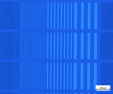
| − | + | [[File: LW-01 S1818Lines 25um Feb2024.png|thumb|right|upright=0.75| 5um, 10um, 25um, and 50um lines using 10mm writehead on 2um S1818 (Feb 2024)]] | |
| − | + | ''Resist on 4" silicon wafer, soft baked at 115C for 60s, development in TMAH 0.26N for 60s. '' <br> | |
| − | {| class="wikitable" | + | <u><small>'''NOTE</u>:'''</small> Even if your resist is listed here, a dose test is always recommended to confirm optimal exposure parameters due to the variability of resist thickness, substrate reflectivity, and the ideal profile for subsequent processes. |
| + | {| class="wikitable" | ||
|- | |- | ||
! Resist | ! Resist | ||
| − | ! Thickness/Spin Speed | + | ! Thickness/<br>Spin Speed |
! Write Head | ! Write Head | ||
! Filter(s) | ! Filter(s) | ||
| Line 141: | Line 132: | ||
| 100 | | 100 | ||
|} | |} | ||
| − | |||
| − | |||
| − | |||
| − | |||
| − | |||
| − | |||
| − | |||
== Resources == | == Resources == | ||
| − | + | ===== SOPs ===== | |
| − | |||
| − | |||
| − | |||
| − | ===== SOPs | ||
* [https://nemo.nano.upenn.edu/media/tool_documents/lw-01-heidelberg-dwl66/LW-01_SOP_v02.pdf SOP] | * [https://nemo.nano.upenn.edu/media/tool_documents/lw-01-heidelberg-dwl66/LW-01_SOP_v02.pdf SOP] | ||
* [https://www.youtube.com/watch?v=q_mvEGSCEGI&list=PLiihbHV9HgpWAcmgdpMGBkejcBhEzoKJO Videos - LW-01 Tool Training] | * [https://www.youtube.com/watch?v=q_mvEGSCEGI&list=PLiihbHV9HgpWAcmgdpMGBkejcBhEzoKJO Videos - LW-01 Tool Training] | ||
* [https://drive.google.com/file/d/1MUMPdLl4GfXtmg3gJjdiPKbdiyCq-elM/view?usp=drive_link Video - Chuck Installation/Removal] | * [https://drive.google.com/file/d/1MUMPdLl4GfXtmg3gJjdiPKbdiyCq-elM/view?usp=drive_link Video - Chuck Installation/Removal] | ||
| − | ===== | + | =====Mask Making===== |
| + | * [https://nemo.nano.upenn.edu/media/tool_documents/lw-01-heidelberg-dwl66/How_to_Make_a_Mask_At_QNF_v05.pdf How to Make a Mask at QNF] | ||
| + | * [https://rise.articulate.com/share/A8k76vtz0l6qxlA2gDZcYHPmJl5bB2C0#/ Introduction to KLayout (LNF)] | ||
| + | * [https://www.youtube.com/playlist?list=PLiihbHV9HgpWZikttBFUh2O8EGUsRu348 BEAMER Training for LW-01] | ||
| + | =====Troubleshooting ===== | ||
* [https://upenn.box.com/s/9kc3fz6gktrrrlac4e0drmzwjzwmufxl Power Up Instructions] | * [https://upenn.box.com/s/9kc3fz6gktrrrlac4e0drmzwjzwmufxl Power Up Instructions] | ||
| + | |||
| + | =====References===== | ||
| + | * [https://heidelberg-instruments.com/product/dwl-66/ Heidelberg Instruments] | ||
Latest revision as of 17:06, 20 November 2025
 |
|
| Tool Name | Heidelberg DWL 66+ Laser Writer |
|---|---|
| Instrument Type | Lithography |
| Staff Manager | Ana Cohen |
| Lab Location | Bay 4 |
| Tool Manufacturer | Heidelberg |
| Tool Model | DWL 66+ |
| NEMO Designation | LW-01 |
| Nearest Phone | 8-9799 |
| SOP Link | SOP |
Description
The fully automated DWL 66+ laser writing system has both binary (2D) and grayscale (2.5D) exposure capability.

The pattern is broken into vertical stripes of ~500px with preset overlap. To write each stripe, the tool modulates and deflects the laser beam based on the provided pattern data while the stage moves along Y. This process repeats along the X direction until the pattern is complete.
Allowed Materials
Substrates
- Mask Plates -- available in the QNF Stockroom pre-coated with AZ1500 and IP3500
- 4" wafers
- Pieceparts > 20mm x 20mm (Starting Aug 2025, DMO system is recommended for small piece part direct write)
Resists -- must be compatible with h-line/ 405nm exposure (Laser exchanged in June 2023. Previous documentation may include 365nm capability.)
Processes
Writehead Selection
NOTE: Pneumatic mode not currently recommended for dry etch and features under 10x listed minimum feature size due to focus issues -- working with Heidelberg service to address.
Last confirmed November 2025.
| Write Head | Optical Focus | Pneumatic Focus | Minimum Feature Size |
|---|---|---|---|
| 10mm | -60 | -100 | 2um |
| 2mm | +50 | -100 | 600nm |
| 40mm | N/A | -100 | 10um |
Exposure Parameters
Mask Plates
530nm resist thickness on chrome-coated soda lime, purchased from TELIC. Development in TMAH 0.26N for 60s. Values last confirmed July 2025.
AZ1500
Lower contrast resist - the default option for most applications
| Write Head | Filter(s) | Laser Power | Intensity |
|---|---|---|---|
| 10mm | 50% | 60 mW | 90 |
| 2mm | 12.5% + 25% | 60 mW | 80 |
| 40mm | NONE | 220 mW | 60 |
IP3500
Higher contrast resist - produces better corners and small pitch gratings
| Write Head | Filter(s) | Laser Power | Intensity |
|---|---|---|---|
| 10mm | NONE | 120 mW | 90 |
| 2mm | 12.5% + 50% | 60 mW | 80 |
Other direct writes
Resist on 4" silicon wafer, soft baked at 115C for 60s, development in TMAH 0.26N for 60s.
NOTE: Even if your resist is listed here, a dose test is always recommended to confirm optimal exposure parameters due to the variability of resist thickness, substrate reflectivity, and the ideal profile for subsequent processes.
| Resist | Thickness/ Spin Speed |
Write Head | Filter(s) | Laser Power | Intensity |
|---|---|---|---|---|---|
| S1805 | 0.5um (3krpm) | 10mm | 50% | 60 mW | 70 |
| S1818 | 2.2um (3krpm) | 10mm | NONE | 130 mW | 100 |

