Difference between revisions of "Oxford PlasmaLab 100 PECVD"
Jump to navigation
Jump to search
| Line 37: | Line 37: | ||
===== Protocols and reports ===== | ===== Protocols and reports ===== | ||
* [https://repository.upenn.edu/scn_tooldata/35/ SiN<sub>x</sub> deposition process parameters] | * [https://repository.upenn.edu/scn_tooldata/35/ SiN<sub>x</sub> deposition process parameters] | ||
| + | * [https://repository.upenn.edu/scn_tooldata/34/ SiO<sub>2</sub> deposition process parameters] | ||
* [https://repository.upenn.edu/scn_tooldata/43/ Optimization of a-Si deposition on Oxford PlasmaLab 100 PECVD using Taguchi L9 based DOE] | * [https://repository.upenn.edu/scn_tooldata/43/ Optimization of a-Si deposition on Oxford PlasmaLab 100 PECVD using Taguchi L9 based DOE] | ||
Revision as of 10:53, 7 April 2022
 |
|
| Tool Name | Oxford PlasmaLab 100 PECVD |
|---|---|
| Instrument Type | Deposition |
| Staff Manager | Sam Azadi |
| Lab Location | Bay 1 |
| Tool Manufacturer | Oxford |
| Tool Model | PlasmaLab 100 |
| NEMO Designation | {{{NEMO_Designation}}} |
| Lab Phone | XXXXX |
| SOP Link | QNF SOP |
Description
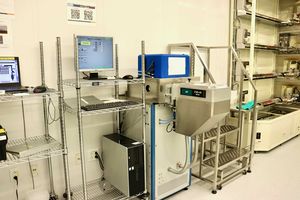
The QNF Oxford Instruments PlasmaLab System 100 Plasma Enhanced Chemical Vapor Deposition (PECVD) tool is used to deposit a variety of thin-film materials at relatively modest temperatures on a variety of substrate materials. The tool utilizes an RF generator to deposit thin films at temperatures lower than traditional chemical vapor deposition systems.
Applications
- Silicon dioxide deposition
- Silicon nitride deposition
- Amorphous silicon deposition
Allowed material in PECVD System
- Si, SixNy, SiO2, SOI
- Hard masks compatible with process temperature
Resources
SOPs & Troubleshooting