Difference between revisions of "Nanoscribe Photonic Professional GT"
(updated materials, configurations information) |
|||
| Line 37: | Line 37: | ||
! Print field radius | ! Print field radius | ||
! Print time (per mm<sup>3</sup>) | ! Print time (per mm<sup>3</sup>) | ||
| − | ! Resins | + | ! Compatible Resins |
| − | ! Substrates | + | ! Compatible Substrates |
|- | |- | ||
| 63x | | 63x | ||
Revision as of 16:59, 7 November 2025
 |
|
| Tool Name | Nanoscribe Photonic Professional GT+ |
|---|---|
| Instrument Type | Lithography |
| Staff Manager | Ana Cohen |
| Lab Location | Bay 6 |
| Tool Manufacturer | Nanoscribe |
| Tool Model | Photonic Professional GT+ |
| NEMO Designation | LW-02 |
| Nearest Phone | XXXXX |
| SOP Link | SOP |
Description
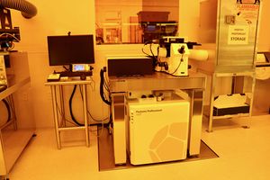
The Nanoscribe Photonic Professional enables the fabrication of true 3D structures in the microscale via two-photon polymerization using a 780nm laser with ~100fs pulse, 80MHz repetition rate. This system allows for cutting-edge research and rapid prototyping in microfluidics, MEMS, microoptics, nanostructures and more.
Upgraded to GT+ in Dec 2024! Includes new housing with easier objective loading with 10x objective capability and greater print height (previously 3mm)
Tool Features
- Laser Power: 50-150mW
- Print Height: Up to 8mm
- Lateral resolution ~ 200 nm
- Vertical resolution ~ 300 nm
- Piezo scanning range: 300 x 300 x 300 μm3
- Stage scanning range: 100 x 100 mm2
Available Print Sets
| Objective | Voxel size (width) | Print field radius | Print time (per mm3) | Compatible Resins | Compatible Substrates |
|---|---|---|---|---|---|
| 63x | ~0.2 μm | 100 μm | ~2.5 hr | IP-Dip, IP-PDMS, IP-L | Fused Silica Glass, ITO/Soda Lime Glass, Silicon |
| 25x | ~0.6 μm | 200 μm | ~1.25 hr | IP-S, IP-PDMS, IP-L, IP-Visio | ITO/Soda Lime Glass, Silicon |
| 10x | ~1.2 μm | 500 μm | ~10 min | IP-Q, IP-PDMS | Silicon |
Voxel = the smallest printable 3D volume, the 3D analogue of a 2D pixel. Single voxels are not mechanically stable. Multiple neighboring voxels/lines are recommended for stable structures.
Print field = the circular region an objective could write without moving the stage. Structures that exceed the print field of the objective must be split into blocks in Describe.
Print time= how long to take to print a 10 μm cube (1 mm3). The print times for the 25x and 10x are calculated for shell recipes. Solid recipes would take longer to print the same volume.
Allowed Materials
Substrates
- 4" Si wafers (~500um thickness)
- Silicon pieces, 25mmx25mmx700um or 25mmx25mmx550um
- Nanoscribe ITO-coated Soda Lime Glass, 25mmx25mmx700um -- available in the QNF Stockroom
- Nanoscribe Fused Silica Glass, 25mmx25mmx700um -- available in the QNF Stockroom
- Borosilicate Coverslips, 30mm x 170um -- for oil immersion configuration
Resists
- IP-Dip
- IP-S
- IP-Q
- IP-PDMS
- IP-L
- IP-Visio
More information about these resists can be found here
Other materials must have tool owner approval before use!
Training Protocol
1. Remote session on EBL-02 for the Describe conversion software, using your structure (90min)
2. In-person session on LW-02 (120min)
3. Qualification session on LW-02, where you run the tool with minimal input (~60min) -- must be done after previous two sessions are completed, cannot be done the same day as the in-person training
All should be requested through NEMO.