Difference between revisions of "Oxford PlasmaLab 100 PECVD"
Jump to navigation
Jump to search
| (44 intermediate revisions by 6 users not shown) | |||
| Line 1: | Line 1: | ||
| − | [[Category:Deposition]] | + | [[Category:Deposition]][[Category:Chemical Vapor Deposition]][[Category:Equipment]] |
| + | |||
{{EquipmentInfo | {{EquipmentInfo | ||
| name = Oxford PlasmaLab 100 PECVD | | name = Oxford PlasmaLab 100 PECVD | ||
| Tool_Name = Oxford PlasmaLab 100 PECVD | | Tool_Name = Oxford PlasmaLab 100 PECVD | ||
| − | | image = [[Image: | + | | image = [[Image:CVD-01.jpeg|300px]] |
| imagecaption = | | imagecaption = | ||
| Instrument_Type = Deposition | | Instrument_Type = Deposition | ||
| − | | Staff_Manager = | + | | Staff_Manager = [[Lucas Barreto | Lucas Barreto]] |
| − | | Lab_Location = Bay | + | | Lab_Location = Bay 1 |
| Tool_Manufacturer = Oxford | | Tool_Manufacturer = Oxford | ||
| Tool_Model = PlasmaLab 100 | | Tool_Model = PlasmaLab 100 | ||
| − | | | + | | NEMO_Designation = CVD-01 |
| − | | Lab_Phone = | + | | Lab_Phone = 215-898-9736 |
| − | | SOP Link = [https://repository.upenn.edu/scn_sop/5/] | + | | SOP Link = [https://repository.upenn.edu/scn_sop/5/ QNF SOP] |
}} | }} | ||
== Description == | == Description == | ||
| − | The QNF | + | The QNF Oxford Instruments PlasmaLab System 100 Plasma Enhanced Chemical Vapor Deposition (PECVD) tool is used to deposit a variety of thin-film materials at relatively modest temperatures on a variety of substrate materials. The tool utilizes an RF generator to deposit thin films at temperatures lower than traditional chemical vapor deposition systems. The tool operates between 150 and 350 C. |
| − | |||
===== Applications ===== | ===== Applications ===== | ||
| − | * Silicon dioxide deposition | + | * [[SiO2 (silicon_dioxide) | Silicon dioxide deposition]] |
* Silicon nitride deposition | * Silicon nitride deposition | ||
| − | * Amorphous silicon deposition | + | * [[Amorphous silicon deposition | Amorphous silicon deposition]] |
===== Allowed material in PECVD System ===== | ===== Allowed material in PECVD System ===== | ||
| − | * Si, Si<sub>x</sub>N<sub>y</sub>, SiO<sub>2</sub>, SOI | + | * Si, Si<sub>x</sub>N<sub>y</sub>, SiO<sub>2</sub>, SOI, SiC, GaN |
| + | * Al, Pt, Cr, W, Mo, Ti | ||
* Hard masks compatible with process temperature | * Hard masks compatible with process temperature | ||
| + | |||
| + | ==== List of materials NOT allowed in the chamber ==== | ||
| + | {| class="wikitable" | ||
| + | |- | ||
| + | ! Name || symbol || Melting Point [C] | ||
| + | |- | ||
| + | | Bismuth || Bi || 271 | ||
| + | |- | ||
| + | | Cadmium || Cd || 321 | ||
| + | |- | ||
| + | | Carbon || C || Subl. | ||
| + | |- | ||
| + | | Gallium || Ga || 30 | ||
| + | |- | ||
| + | | Gold || Au || 1062 | ||
| + | |- | ||
| + | | Indium || In || 157 | ||
| + | |- | ||
| + | | Lead || Pb || 328 | ||
| + | |- | ||
| + | | Lithium || Li || 179 | ||
| + | |- | ||
| + | | Selenium || Se || 217 | ||
| + | |- | ||
| + | | Sulfur || S || 115 | ||
| + | |- | ||
| + | | Tellurium || Te || 452 | ||
| + | |- | ||
| + | | Thallium || Tl || 302 | ||
| + | |- | ||
| + | | Tin || Sn || 232 | ||
| + | |- | ||
| + | | Zinc || Zn || 419 | ||
| + | |} | ||
| + | |||
| + | == Process information == | ||
| + | |||
| + | |||
| + | === Standard process data - Table temperature fixed at 350 C === | ||
| + | * SiO<sub>2</sub> on 10/10/2025 | ||
| + | |||
| + | : Recipe parameters: optimized process parameters are in the report under "Protocols and Reports" section | ||
| + | |||
| + | : Recipe name on the tool: Test-SiO2 | ||
| + | |||
| + | : Deposition rate: ~ 323.17 nm/min ± 1.75 nm/min | ||
| + | |||
| + | : [[SiO2_Deposition_Process_Data|SiO<sub>2</sub> Process Data]] | ||
| + | |||
| + | |||
| + | |||
| + | * SiNx on 07/29/2024 | ||
| + | |||
| + | : Recipe parameters: optimized process parameters are in the report under "Protocols and Reports" section | ||
| + | |||
| + | : Recipe name on the tool: Test-SiNx deposition | ||
| + | |||
| + | : Deposition rate: ~ 46 nm/min ± 2 nm/min | ||
| + | |||
| + | |||
| + | |||
| + | * a-Si on 01/09/2024 | ||
| + | |||
| + | : Recipe parameters: optimized process parameters are in the report under "Protocols and Reports" section | ||
| + | |||
| + | : Recipe name on the tool: a-Si | ||
| + | |||
| + | : Deposition rate: ~ 60 nm/min ± 5 nm/min | ||
| + | |||
| + | |||
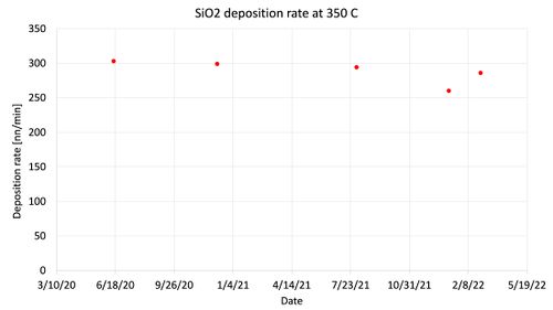
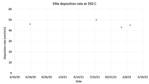
| + | ==== Deposition Rate Monitoring ==== | ||
| + | [[Image:Sio2 dep on cvd-01.jpg|left|500px]] [[Image:Sinx dep rate on cvd-01.jpg|center|500px]] | ||
| + | |||
| + | === Special process data - adjustable table temperature === | ||
| + | * SiO2 | ||
| + | |||
| + | Recipe parameters: optimized process parameters are in the report under "Protocols and Reports" section - table temperature at 200 C | ||
| + | |||
| + | Recipe name on the tool: Test-SiO2 | ||
| + | |||
| + | Deposition rate: ~ 230 nm/min ± 2 nm/min | ||
== Resources == | == Resources == | ||
===== SOPs & Troubleshooting ===== | ===== SOPs & Troubleshooting ===== | ||
| − | * [https://repository.upenn.edu/scn_sop/ | + | * [https://repository.upenn.edu/scn_sop/5/ QNF SOP] |
| − | + | * [https://upenn.box.com/s/sglgbidfjpw36f6v50rzgcpll5yliloc/ PECVD Table Temp Tuning Procedure] | |
| − | ===== Protocols ===== | + | ===== Protocols and Reports ===== |
| − | * [https://repository.upenn.edu/scn_tooldata/35/ | + | * [https://repository.upenn.edu/scn_tooldata/34/ SiO<sub>2</sub> deposition process parameters] |
| + | * [https://repository.upenn.edu/scn_tooldata/35/ SiN<sub>x</sub> deposition process parameters] | ||
| + | * [https://repository.upenn.edu/scn_tooldata/43/ Optimization of a-Si deposition on Oxford PlasmaLab 100 PECVD using Taguchi L9 based DOE] | ||
Latest revision as of 13:38, 21 October 2025
 |
|
| Tool Name | Oxford PlasmaLab 100 PECVD |
|---|---|
| Instrument Type | Deposition |
| Staff Manager | Lucas Barreto |
| Lab Location | Bay 1 |
| Tool Manufacturer | Oxford |
| Tool Model | PlasmaLab 100 |
| NEMO Designation | CVD-01 |
| Nearest Phone | 215-898-9736 |
| SOP Link | QNF SOP |
Description
The QNF Oxford Instruments PlasmaLab System 100 Plasma Enhanced Chemical Vapor Deposition (PECVD) tool is used to deposit a variety of thin-film materials at relatively modest temperatures on a variety of substrate materials. The tool utilizes an RF generator to deposit thin films at temperatures lower than traditional chemical vapor deposition systems. The tool operates between 150 and 350 C.
Applications
- Silicon dioxide deposition
- Silicon nitride deposition
- Amorphous silicon deposition
Allowed material in PECVD System
- Si, SixNy, SiO2, SOI, SiC, GaN
- Al, Pt, Cr, W, Mo, Ti
- Hard masks compatible with process temperature
List of materials NOT allowed in the chamber
| Name | symbol | Melting Point [C] |
|---|---|---|
| Bismuth | Bi | 271 |
| Cadmium | Cd | 321 |
| Carbon | C | Subl. |
| Gallium | Ga | 30 |
| Gold | Au | 1062 |
| Indium | In | 157 |
| Lead | Pb | 328 |
| Lithium | Li | 179 |
| Selenium | Se | 217 |
| Sulfur | S | 115 |
| Tellurium | Te | 452 |
| Thallium | Tl | 302 |
| Tin | Sn | 232 |
| Zinc | Zn | 419 |
Process information
Standard process data - Table temperature fixed at 350 C
- SiO2 on 10/10/2025
- Recipe parameters: optimized process parameters are in the report under "Protocols and Reports" section
- Recipe name on the tool: Test-SiO2
- Deposition rate: ~ 323.17 nm/min ± 1.75 nm/min
- SiNx on 07/29/2024
- Recipe parameters: optimized process parameters are in the report under "Protocols and Reports" section
- Recipe name on the tool: Test-SiNx deposition
- Deposition rate: ~ 46 nm/min ± 2 nm/min
- a-Si on 01/09/2024
- Recipe parameters: optimized process parameters are in the report under "Protocols and Reports" section
- Recipe name on the tool: a-Si
- Deposition rate: ~ 60 nm/min ± 5 nm/min
Deposition Rate Monitoring


Special process data - adjustable table temperature
- SiO2
Recipe parameters: optimized process parameters are in the report under "Protocols and Reports" section - table temperature at 200 C
Recipe name on the tool: Test-SiO2
Deposition rate: ~ 230 nm/min ± 2 nm/min