Difference between revisions of "EVG 510 Wafer Bonder"
Jump to navigation
Jump to search
(update to NEMO) |
|||
| (One intermediate revision by one other user not shown) | |||
| Line 7: | Line 7: | ||
| imagecaption = | | imagecaption = | ||
| Instrument_Type = Back End | | Instrument_Type = Back End | ||
| − | | Staff_Manager = Eric Johnston | + | | Staff_Manager = [[Eric Johnston | Eric Johnston]] |
| − | | Lab_Location = Bay | + | | Lab_Location = Bay 4 |
| Tool_Manufacturer = EV Group | | Tool_Manufacturer = EV Group | ||
| Tool_Model = 510 | | Tool_Model = 510 | ||
| − | | | + | | NEMO_Designation = BE-01 |
| Lab_Phone = XXXXX | | Lab_Phone = XXXXX | ||
| SOP Link = [https://www.seas.upenn.edu/~nanosop/Wafer_Bonder_SOP.htm SOP] | | SOP Link = [https://www.seas.upenn.edu/~nanosop/Wafer_Bonder_SOP.htm SOP] | ||
Latest revision as of 13:22, 3 January 2024
 |
|
| Tool Name | EVG 510 Wafer Bonder |
|---|---|
| Instrument Type | Back End |
| Staff Manager | Eric Johnston |
| Lab Location | Bay 4 |
| Tool Manufacturer | EV Group |
| Tool Model | 510 |
| NEMO Designation | BE-01 |
| Lab Phone | XXXXX |
| SOP Link | SOP |
Description
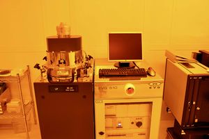
The EVG510 Wafer Bonding System is a highly flexible R&D system that can handle small substrate pieces up to 100 mm wafers. The new tool supports a variety of bonding processes, such as anodic, eutectic, diffusion, fusion, solder, and adhesive bonds, as well as other thermal processes, including oxide removal and high temperature bakes under a controlled atmosphere. The system also offers quick re-tooling with a conversion time of less than five minutes, making it ideal for universities and R&D as well as small-volume production applications.
Specification Maximum contact force: 10 kN Maximum temperature: 550 ºC Vacuum: ~0.1 mbar Power supply for anodic bonding: 0-2000 V and 50 mA
Applications
- Anodic wafer bonding
- Eutectic wafer bonding
- Diffusion wafer bonding
- Fusion wafer bonding
- Adhesive wafer bonding