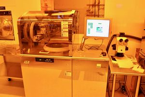
Difference between revisions of "SUSS MicroTec AS8 AltaSpray"
Jump to navigation
Jump to search
m (Changed protection level for "SUSS MicroTec AS8 AltaSpray" ([Edit=Allow only autoconfirmed users] (indefinite) [Move=Allow only autoconfirmed users] (indefinite))) |
|||
| Line 24: | Line 24: | ||
== Resources == | == Resources == | ||
| + | |||
| + | ===== Process characterization and tool data ===== | ||
| + | * [https://repository.upenn.edu/scn_tooldata/46/ Influence of flow rate, nozzle speed, pitch and the number of passes on the thickness of S1805 photoresist in SUSS MicroTec AS8 spray coater] | ||
| + | |||
===== SOPs & Troubleshooting ===== | ===== SOPs & Troubleshooting ===== | ||
* [https://www.seas.upenn.edu/~nanosop/SprayCoater_SOP.htm QNF SOP] | * [https://www.seas.upenn.edu/~nanosop/SprayCoater_SOP.htm QNF SOP] | ||
Revision as of 11:33, 28 November 2022
 |
|
| Tool Name | SUSS MicroTec AS8 AltaSpray |
|---|---|
| Instrument Type | Lithography |
| Staff Manager | David Jones |
| Lab Location | Bay 2 |
| Tool Manufacturer | SUSS MicroTec |
| Tool Model | AS8 AltaSpray |
| NEMO Designation | {{{NEMO_Designation}}} |
| Lab Phone | XXXXX |
| SOP Link | SOP |
Description
SUSS MicroTec’s proprietary AltaSpray coating technology is a unique resist deposition method that is capable of producing highly uniform resist films on different 3-D microstructures. The AltaSpray technology is capable of coating 90° corners, KOH etched cavities, Through Silicon Vias (TSVs) or lenses with topographies ranging from a few micron to 600µm or more. The ability to produce conformal resist coatings on severe topography makes them the ideal choice for R&D, MEMS, 3D-Integration and Wafer Level Packaging applications like 3D image sensor packaging. Wafer sizes from pieces to 200mm.
Applications
- Automated resist spray coater for high topographies
Resources
Process characterization and tool data