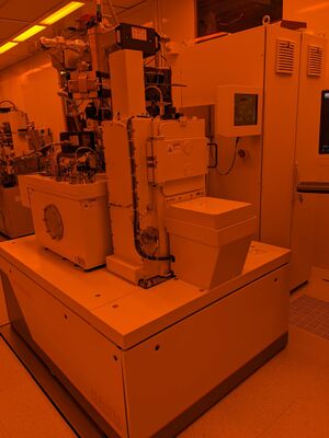
Difference between revisions of "Raith EBPG5200+ E-Beam Lithography System"
Jump to navigation
Jump to search
(update to NEMO) |
|||
| Line 32: | Line 32: | ||
===== SOPs & Troubleshooting ===== | ===== SOPs & Troubleshooting ===== | ||
* [https://repository.upenn.edu/entities/publication/8cf0d00b-4111-444b-90d1-965b23691703 SOP] | * [https://repository.upenn.edu/entities/publication/8cf0d00b-4111-444b-90d1-965b23691703 SOP] | ||
| − | |||
* [https://upenn.box.com/s/atymr3okn3xf20rb1kvk7ny79plojobm Graph of Spotsize vs. Current (Internal Use Only)] | * [https://upenn.box.com/s/atymr3okn3xf20rb1kvk7ny79plojobm Graph of Spotsize vs. Current (Internal Use Only)] | ||
Revision as of 17:07, 3 January 2024
 |
|
| Tool Name | Raith EBPG5200+ EBL |
|---|---|
| Instrument Type | Lithography |
| Staff Manager | David Barth |
| Lab Location | Bay 4 |
| Tool Manufacturer | Raith |
| Tool Model | EBPG5200+ |
| NEMO Designation | EBL-03 |
| Lab Phone | 8-9799 |
| SOP Link | SOP |
Description
The Raith EBPG5200+ is an electron beam lithography tool capable of high resolution patterning at 100 kV. It has a 125 MHz pattern generator, a maximum current of 350 nA, and a 1 mm mainfield size. It has an automatic aperture changer, automatic and dynamic focus and stigmation, and automatic alignment. The EBPG can achieve linewidths <8nm with stitching and overlay accuracy better than 10nm.
Applications
- Large scale, high speed patterning of positive and negative e-beam resists with features from <10 nm to micron/mm scale
Allowed Materials
- Standard semiconductor materials
- Low vapor pressure metals
- Resists