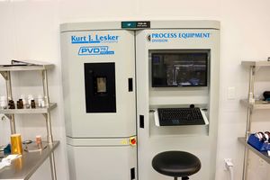
Lesker PVD75 DC/RF Sputterer
Jump to navigation
Jump to search
 |
|
| Tool Name | Lesker PVD75 DC/RF Sputterer |
|---|---|
| Instrument Type | Deposition |
| Staff Manager | David Barth |
| Lab Location | Bay 2 |
| Tool Manufacturer | Kurt J. Lesker |
| Tool Model | PVD75 |
| NEMO Designation | {{{NEMO_Designation}}} |
| Lab Phone | XXXXX |
| SOP Link | SOP |
Tool description
The Kurt J. Lesker PVD75 Sputter system is configured with 4 sputter guns in the following configuration:
Target 1: RF power, insulating/conductive target
Target 2: DC power, magnetic/non-magnetic conductive target
Target 3: DC power, non-magnetic conductive target
Target 4: DC power, magnetic/non-magnetic conductive target
The system is cryo-pumped process chamber with an automated interface, wafer platen rotation and heating up to 550°C, accepting sample sized from pieces to 150 mm diameter wafers.
When choosing between PVD-03 and PVD-05, consider the following:
- PVD-03 is a load-locked system so base pressure will be better (~5e-8 torr vs. ~5e-6 torr) and pumpdown times will be much faster compared with PVD-05, which is an open load system.
- PVD-03 can handle one 6" wafer or one 4" wafer (or several smaller pieces) per run. PVD-05 has a large platen and can accept about four 4" wafers with good uniformity.
- PVD-03 is in a sputter up configuration, which means the guns point up and the sample must be attached upside down. This is usually considered cleaner, but requires greater consideration for sample mounting. PVD-05 is in sputter down configuration, so samples can just be placed on the platen.
- Magnetic materials can only be sputtered from PVD-03. PVD-05 does not have the necessary high mag sources
Deposition sources
Metals
- Ag (Warning! Ag target must be cooled down for more than 15 min after deposition)
- Al
- Au
- Co
- Cr
- Cu
- Fe
- Mn
- Mo
- Nb
- Ni
- Pd
- Pt
- Ti
- W
Semiconductors & metalloids
- Ge
- Sb
- Si
- p-Si (boron-doped)
Oxides, fluorides & nitrides
- Al2O3
- AZO (ZnO2/Al2O3; transparent conductive oxide)
- ITO (indium-doped tin oxide; transparent conductive oxide)
- MgF2
- MgO
- NbN
- Si3N4
- SiO2
- Ta2O5
- TiO2
- TiN
Alloys & ceramics
- Al/Si (99/1)
- Fe/Ge (81/19 & 83/17)
- Ni/Fe
- Ni/Cr (80/20)
- YSZ (Yttria-stabilized zirconia)
Other targets
- Please consult with staff
Resources
SOPs & Troubleshooting
Process Data
- Note: The sputter yield chart can be useful for estimating approximately what rate to expect from materials, but the rate given is highly dependent on tool configuration and is not directly relevant