Difference between revisions of "Raith EBPG5200+ E-Beam Lithography System"
Jump to navigation
Jump to search
| (9 intermediate revisions by 2 users not shown) | |||
| Line 13: | Line 13: | ||
| NEMO_Designation = EBL-03 | | NEMO_Designation = EBL-03 | ||
| Lab_Phone = 8-9799 | | Lab_Phone = 8-9799 | ||
| − | | SOP Link = [ | + | | SOP Link = [[Media:EBPG5200+_SOP.pdf | SOP]] |
}} | }} | ||
| Line 26: | Line 26: | ||
* Standard semiconductor materials | * Standard semiconductor materials | ||
* Low vapor pressure metals | * Low vapor pressure metals | ||
| − | * Resists | + | * Resists |
| + | ** [https://wiki.nano.upenn.edu/wiki/index.php?title=Resists_at_QNF#Standard_e-beam_Resists Standard e-beam resists] | ||
| + | ** [https://wiki.nano.upenn.edu/wiki/index.php?title=Resists_at_QNF#Stockroom_e-beam_Resists Stockroom e-beam resists] | ||
| + | ** [https://wiki.nano.upenn.edu/wiki/index.php?title=Resists_at_QNF#Other_Resists PMGI] | ||
== Resources == | == Resources == | ||
| − | ===== | + | ===== SOP ===== |
| − | * [ | + | <pdf height="800"> File:EBPG5200+_SOP.pdf</pdf> |
| + | |||
| + | ===== Useful Information ===== | ||
| + | * [[Media:EBPG5200+_SOP.pdf | SOP]] | ||
* [https://upenn.box.com/s/atymr3okn3xf20rb1kvk7ny79plojobm Graph of Spotsize vs. Current (Internal Use Only)] | * [https://upenn.box.com/s/atymr3okn3xf20rb1kvk7ny79plojobm Graph of Spotsize vs. Current (Internal Use Only)] | ||
| + | * [https://upenn.box.com/s/gzj28stdehm1kfmwjpcnio7vimr4m1w9 Alignment Mark Guidelines] | ||
===== Resist and Process Data ===== | ===== Resist and Process Data ===== | ||
| Line 40: | Line 47: | ||
* [https://avs.scitation.org/doi/full/10.1116/1.2366698 Cold Development for PMMA and ZEP] | * [https://avs.scitation.org/doi/full/10.1116/1.2366698 Cold Development for PMMA and ZEP] | ||
* [https://www.sciencedirect.com/science/article/pii/S0167931702004689 IPA:H<sub>2</sub>O for High Contrast Development of PMMA] | * [https://www.sciencedirect.com/science/article/pii/S0167931702004689 IPA:H<sub>2</sub>O for High Contrast Development of PMMA] | ||
| + | * [[ZEP_Process_Data | ZEP520A Contrast Curve]] | ||
Latest revision as of 14:12, 6 November 2024
 |
|
| Tool Name | Raith EBPG5200+ EBL |
|---|---|
| Instrument Type | Lithography |
| Staff Manager | David Barth |
| Lab Location | Bay 4 |
| Tool Manufacturer | Raith |
| Tool Model | EBPG5200+ |
| NEMO Designation | EBL-03 |
| Lab Phone | 8-9799 |
| SOP Link | SOP |
Description
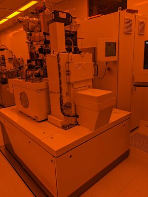
The Raith EBPG5200+ is an electron beam lithography tool capable of high resolution patterning at 100 kV. It has a 125 MHz pattern generator, a maximum current of 350 nA, and a 1 mm mainfield size. It has an automatic aperture changer, automatic and dynamic focus and stigmation, and automatic alignment. The EBPG can achieve linewidths <8nm with stitching and overlay accuracy better than 10nm.
Applications
- Large scale, high speed patterning of positive and negative e-beam resists with features from <10 nm to micron/mm scale
Allowed Materials
- Standard semiconductor materials
- Low vapor pressure metals
- Resists
Resources
SOP