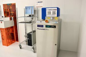
Difference between revisions of "Oxford 80 Plus RIE"
Jump to navigation
Jump to search
| (34 intermediate revisions by 2 users not shown) | |||
| Line 7: | Line 7: | ||
| imagecaption = | | imagecaption = | ||
| Instrument_Type = Etch | | Instrument_Type = Etch | ||
| − | | Staff_Manager = Sam Azadi | + | | Staff_Manager = [[Sam Azadi | Sam Azadi]] |
| Lab_Location = Bay 2 | | Lab_Location = Bay 2 | ||
| Tool_Manufacturer = Oxford Instruments | | Tool_Manufacturer = Oxford Instruments | ||
| Tool_Model = 80+ | | Tool_Model = 80+ | ||
| − | | | + | | NEMO_Designation = DE-04 |
| Lab_Phone = 215-898-9748 | | Lab_Phone = 215-898-9748 | ||
| SOP Link = [https://repository.upenn.edu/scn_sop/7/ QNF SOP] | | SOP Link = [https://repository.upenn.edu/scn_sop/7/ QNF SOP] | ||
| Line 27: | Line 27: | ||
* Etch of resist | * Etch of resist | ||
| − | + | ===== The following materials are ''NOT'' allowed in the chamber ===== | |
| − | ===== The following materials are | + | - Au, Ag, PZT, Pt, ZnO, ITO, Pb, Zn, In, Ni, Fe, Cu |
| − | - Au, Ag, PZT, ZnO, ITO, Pb, Zn, In | ||
===== The following materials can not be exposed to plasma in the chamber ===== | ===== The following materials can not be exposed to plasma in the chamber ===== | ||
| Line 36: | Line 35: | ||
== Standard Process Information == | == Standard Process Information == | ||
| − | ==== | + | ==== Etch Rate ==== |
| − | + | Recipe parameters are defined in the reports above. - all rates are calculated from a full 4" wafers, small features may have lower etch rate. | |
| + | |||
| + | Etch rate of... | ||
| + | |||
| + | * '''PECVD oxide and nitride''' are listed in the ''reports below''. | ||
| + | * '''thermal SiO2''' using '''CF4 recipe''': ''48 nm/min'' | ||
| + | * '''thermal SiO2''' using '''CHF3/O2 recipe''': ''45 nm/min'' | ||
| + | * '''LPCVD SiNx''' using '''CF4 recipe''': ''60 nm/min'', DC bias 420 V - measured on 07/29/2024 | ||
| + | * '''LPCVD SiNx''' using '''CHF3/O2 recipe''': ''45 nm/min'', DC bias 410 V - measured on 03/05/2024 | ||
| + | |||
| + | |||
| + | |||
| + | |||
| + | [[ PECVD SiO2 via CHF3 + O2 | '''PECVD SiO<sub>2</sub> via CHF<sub>3</sub> + O <sub>2</sub> ''']] | ||
| + | |||
| + | [[ PECVD SiNx via CHF3 + O2 | '''PECVD SiN<sub>x</sub> via CHF<sub>3</sub> + O <sub>2</sub>''']] | ||
| + | |||
| + | == Resources == | ||
| − | |||
* [https://repository.upenn.edu/scn_tooldata/37/ '''PECVD SiN<sub>x</sub> via CF<sub>4</sub>'''] | * [https://repository.upenn.edu/scn_tooldata/37/ '''PECVD SiN<sub>x</sub> via CF<sub>4</sub>'''] | ||
| Line 52: | Line 67: | ||
* [https://repository.upenn.edu/scn_protocols/55/ ''' Comparison of Si and PECVD SiO<sub>2</sub> via CF<sub>4</sub> and CHF<sub>3</sub> + O <sub>2</sub>'''] | * [https://repository.upenn.edu/scn_protocols/55/ ''' Comparison of Si and PECVD SiO<sub>2</sub> via CF<sub>4</sub> and CHF<sub>3</sub> + O <sub>2</sub>'''] | ||
| − | |||
| − | |||
| − | |||
| − | |||
| − | |||
| − | |||
| − | |||
| − | |||
| − | |||
| − | |||
| − | |||
| − | |||
| − | |||
| − | |||
| − | |||
===== SOPs & Troubleshooting ===== | ===== SOPs & Troubleshooting ===== | ||
Latest revision as of 15:08, 16 October 2024
 |
|
| Tool Name | Oxford 80 Plus RIE |
|---|---|
| Instrument Type | Etch |
| Staff Manager | Sam Azadi |
| Lab Location | Bay 2 |
| Tool Manufacturer | Oxford Instruments |
| Tool Model | 80+ |
| NEMO Designation | DE-04 |
| Lab Phone | 215-898-9748 |
| SOP Link | QNF SOP |
Description
Oxford 80 Plus is an anisotropic dry etch tool. The main use of this tool is to etch SiO2, and SiNx to create hard masks for deep Si etch. However, it etches many other materials, including a variety of resists. The tool is connected to the following gases: Ar, O2, CF4, CHF3, SF6.
The plasma is ignited by the oscillating electric field created by the RF power at 13.56 MHz. The wafer is cooled down via passive cooling through a graphite chuck.
Applications
- Etch of SiO2
- Etch of SiNx
- Etch of Si
- Etch of resist
The following materials are NOT allowed in the chamber
- Au, Ag, PZT, Pt, ZnO, ITO, Pb, Zn, In, Ni, Fe, Cu
The following materials can not be exposed to plasma in the chamber
- SU-8, Cyclone, Polyimide
Standard Process Information
Etch Rate
Recipe parameters are defined in the reports above. - all rates are calculated from a full 4" wafers, small features may have lower etch rate.
Etch rate of...
- PECVD oxide and nitride are listed in the reports below.
- thermal SiO2 using CF4 recipe: 48 nm/min
- thermal SiO2 using CHF3/O2 recipe: 45 nm/min
- LPCVD SiNx using CF4 recipe: 60 nm/min, DC bias 420 V - measured on 07/29/2024
- LPCVD SiNx using CHF3/O2 recipe: 45 nm/min, DC bias 410 V - measured on 03/05/2024