Difference between revisions of "Lesker PVD75 DC/RF Sputterer"
Jump to navigation
Jump to search
m |
|||
| Line 55: | Line 55: | ||
===== SOPs & Troubleshooting ===== | ===== SOPs & Troubleshooting ===== | ||
* [https://www.seas.upenn.edu/~nanosop/PVD75_Sputtering_SOP.htm SOP] | * [https://www.seas.upenn.edu/~nanosop/PVD75_Sputtering_SOP.htm SOP] | ||
| + | |||
| + | * [https://upenn.box.com/s/duex4o7xnhoq4dbqoo51aaij1o1b44mk PVD-03 Open Load SOP] | ||
===== Process Data ===== | ===== Process Data ===== | ||
* [https://upenn.box.com/s/lujbua3msga3313fntajkw3bcwh0d63w PVD-03 Recipes] | * [https://upenn.box.com/s/lujbua3msga3313fntajkw3bcwh0d63w PVD-03 Recipes] | ||
Revision as of 10:32, 27 May 2022
 |
|
| Tool Name | Lesker PVD75 DC/RF Sputterer |
|---|---|
| Instrument Type | Deposition |
| Staff Manager | David Barth |
| Lab Location | Bay 2 |
| Tool Manufacturer | Kurt J. Lesker |
| Tool Model | PVD75 |
| NEMO Designation | {{{NEMO_Designation}}} |
| Lab Phone | XXXXX |
| SOP Link | SOP |
Description
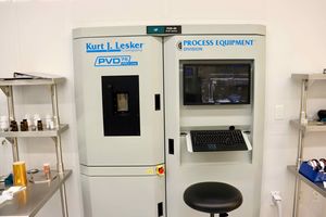
The Kurt J. Lesker PVD75 Sputter system is configured with 4 sputter guns in the following configuration:
Target 1: RF power, insulating/conductive target
Target 2: DC power, magnetic/non-magnetic conductive target
Target 3: DC power, non-magnetic conductive target
Target 4: DC power, magnetic/non-magnetic conductive target
The system is cryo-pumped process chamber with an automated interface, wafer platen rotation and heating up to 550°C, accepting sample sized from pieces to 150 mm diameter wafers.
Deposition Sources
- ITO
- Cr
- Ni
- Fe
- FeGa
- NiFe
- Ti
- Ni
- Cu
- Al
- SiO2
- TiO2
- Al2O3
- Ge
- Pt
- Ag (Warning! Ag target must be cooled down for more than 15 min after depositing Ag film.)
- Pd
- Si
- Mo
- Various others - please consult with staff